Photoresists are light-sensitive materials essential for creating patterns on silicon wafers during semiconductor manufacturing. There are two main types: positive photoresists and negative photoresists. The choice between them depends on factors like resolution, adhesion, sensitivity, and process requirements.
- Positive photoresists dissolve in exposed areas when exposed to UV light, achieving finer resolutions (down to 20 nm) and sharper patterns. They work best for advanced nodes under 45 nm but require precise environmental controls and surface preparation.
- Negative photoresists harden in exposed regions, offering stronger adhesion and a broader process window. They are better suited for applications like MEMS and wafer-level packaging, where durability and thicker films are needed.
Quick Comparison:
| Feature | Positive Photoresist | Negative Photoresist |
|---|---|---|
| Resolution | ~20 nm | ~40 nm |
| Adhesion | Fair (requires primer) | Excellent |
| Exposure Dose | 100–150 mJ/cm² | 300–400 mJ/cm² |
| Depth of Focus (DOF) | ~0.5 µm | ~1.2 µm |
| Cost | Higher | Lower |
Positive resists are ideal for high-precision, small-scale patterns, while negative resists excel in durability and flexibility for thicker structures. Your choice depends on the specific requirements of your semiconductor process.
Positive vs. Negative Photoresists: Key Specs Compared
Positive vs Negative vs Image Reversal Photoresist: Key Differences Explained
sbb-itb-aa4586a
1. Positive Photoresists
Positive photoresists play a central role in advanced semiconductor manufacturing, particularly for nodes smaller than 45 nm. When exposed to UV light, the exposed areas degrade, becoming soluble and leaving behind a precise pattern.
Resolution
These resists can achieve feature resolutions as small as 20 nm, which is about half the smallest feature size possible with negative resists [2]. This is due to their higher contrast values (γ = 0.3–0.5), allowing for sharper pattern edges and more accurate replication of the design [2][5]. Additionally, positive resists don’t swell during development, ensuring stability at the nanometer scale [3].
Adhesion
Adhesion is dependable for fine patterns but requires careful surface preparation. A common method involves applying an HMDS (Hexamethyldisilazane) primer before coating to promote uniform bonding with the substrate [2]. Following this, a soft bake at 90°C on a temperature-controlled hot plate removes residual solvents and enhances adhesion [2]. Skipping these steps can lead to adhesion issues, particularly on negatively charged surfaces.
Sensitivity
Positive resists require lower exposure doses, typically 100–150 mJ/cm², compared to the 300–400 mJ/cm² needed for negative resists [2]. This lower energy demand speeds up production and reduces energy use per wafer. Many modern positive resists incorporate chemical amplification (CAR), where a single photogenerated acid molecule triggers a chain reaction of deprotection, amplifying the effect of absorbed photons [6].
Process Robustness
The high resolution of positive resists comes with a narrower process window. For example, their depth of focus (DOF) is about 0.5 µm, much smaller than the 1.2 µm DOF of negative resists [2]. This requires tight environmental controls, such as a Class 100 cleanroom maintained at 68±2°F (21±1°C) and 45±5% relative humidity [2]. Exposure dose variations must also stay within ±5% to ensure precise critical dimension (CD) control [2]. While these strict controls add complexity, the enhanced resolution makes the effort worthwhile. Next, we’ll look at how negative photoresists stack up in these areas.
2. Negative Photoresists
Negative photoresists work by hardening when exposed to UV light. This process involves cross-linking polymer chains, creating an insoluble network that remains intact after development. The unexposed areas are removed during development, leaving behind the hardened pattern.
Resolution
Negative resists can resolve features as small as 40 nm [2]. However, the cross-linking mechanism can cause the polymer network to spread slightly beyond the exposure boundary, leading to less defined pattern edges. Their contrast value (γ) ranges from 1.5 to 2.5, which is lower than the 2.5–3.5 contrast range of positive resists. This results in softer edges but is an acceptable trade-off for applications like MEMS and wafer-level packaging, where thick films and high-aspect-ratio structures are more important than achieving sub-20 nm precision [1].
Adhesion
One of the standout features of negative resists is their superior adhesion. The cross-linking reaction forms a dense polymer network that bonds tightly to the substrate, providing much stronger adhesion than positive resists [2].
"Negative resists provide robustness and the ability to support thicker films, making negative resists ideal for applications that require enhanced adhesion and structural integrity." – Wevolver [2]
This strong adhesion helps prevent pattern collapse, a common issue in high-aspect-ratio features caused by capillary forces during development [2]. To avoid collapse, engineers often aim for aspect ratios below 3:1 [2]. Additionally, negative resists are resistant to harsh chemicals used in etching and electroplating, making them suitable for creating durable, long-lasting structures [1][7].
Sensitivity
Negative resists require higher energy for exposure compared to positive resists. A complete cross-linking reaction typically needs 300–400 mJ/cm², reflecting their lower quantum yield of 0.5–0.7 [2]. Development is also slower, occurring at rates of 50–100 nm/s, compared to 150–200 nm/s for positive resists [2]. However, dark loss – unintended thinning of unexposed areas – remains minimal at 1–3 nm/min [2]. These characteristics make negative resists more forgiving during processing, contributing to their operational reliability.
Process Robustness
The process robustness of negative resists makes them a strong choice for manufacturing. Their depth of focus (DOF) of ~1.2 µm provides more flexibility in handling variations in the imaging plane or uneven wafer surfaces, compared to the 0.5 µm DOF of positive resists [2]. Additionally, their higher glass transition temperature (Tg of 150–180°C) allows them to withstand the thermal stress of downstream fabrication steps [2]. For high-volume production, this wider process window ensures consistent performance across different manufacturing conditions.
Pros and Cons
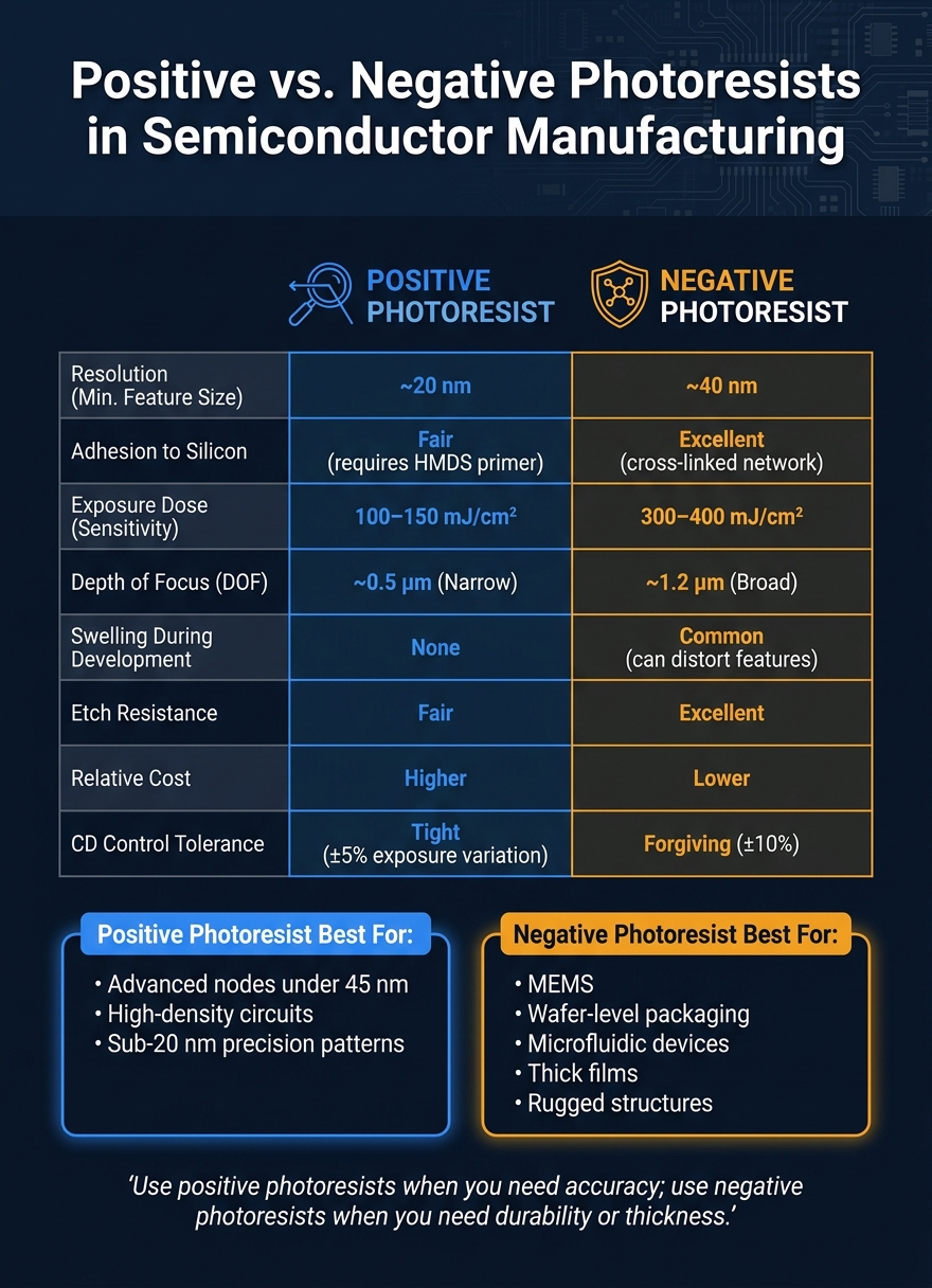
Positive and negative photoresists each bring distinct advantages to semiconductor processes, with the choice largely depending on specific application needs. Positive resists are known for their fine resolution, while negative resists stand out for their durability and broader process flexibility. The table below summarizes their key differences:
| Characteristic | Positive Photoresist | Negative Photoresist |
|---|---|---|
| Resolution (min. feature size) | ~20 nm – ideal for advanced (sub–45 nm) nodes [2] | ~40 nm – suitable for MEMS and wafer-level packaging [2] |
| Adhesion to silicon | Fair (often requires an HMDS primer) [4] | Excellent – cross‐linked network bonds tightly [4] |
| Sensitivity (exposure dose) | 100–150 mJ/cm² – faster exposure [2] | 300–400 mJ/cm² – requires more energy [2] |
| Depth of focus (DOF) | Narrow – ~0.5 µm [2] | Broad – ~1.2 µm [2] |
| Swelling during development | None [3] | Common – can distort fine features [4] |
| Etch resistance | Fair [4] | Excellent [4] |
| Relative cost | Higher [8] | Lower [8] |
| CD control tolerance | Tight – within ±5% exposure variation [2] | More forgiving – allows ±10% [2] |
This side-by-side comparison helps clarify which resist type best suits specific semiconductor needs.
Positive resists work with aqueous developers, such as TMAH, which selectively remove exposed regions. This eliminates swelling and ensures patterns remain sharp. Muhammad Hassaan from the University of South-Eastern Norway highlights their benefits:
"Positive photoresists offer several key benefits, including superior resolution, high contrast, enhanced etch resistance, absence of swelling behavior during development, better edge resolution, and improved aspect ratios of structures." [3]
On the other hand, negative resists use organic developers that can affect both exposed and unexposed areas. This often causes swelling, which may blur pattern edges, making them less suitable for advanced front-end processes. However, their strengths shine in applications requiring thicker films and chemical resilience, such as wafer-level packaging and microfluidic devices. Shin-Etsu MicroSi explains:
"Negative resists are a great material to use for those semiconductor supplies that don’t require such high resolutions… [they] have a faster photo speed, wider process latitude and a significantly lower operating cost." [8]
Both types play crucial roles in semiconductor manufacturing, with their selection depending on the trade-offs between resolution, cost, and process requirements.
Disclaimer: This content is for informational purposes only. Consult official regulations and qualified professionals before making sourcing or formulation decisions.
Conclusion
The decision between positive and negative photoresists hinges on your priorities – precision or durability. As Alfa Chemistry puts it: "Use positive photoresists when you need accuracy; Use negative photoresists when you need durability or thickness." [1]
For advanced semiconductor nodes under 45 nm, positive resists achieve sub-20 nm resolution and maintain high pattern fidelity – essential for intricate, high-density circuits [2]. On the other hand, negative resists excel in adhesion, offer a broader 1.2 µm depth of focus, and are cost-effective, making them ideal for MEMS, wafer-level packaging, and rugged structural applications [2][8]. This trade-off highlights the need for tailored material selection based on specific manufacturing goals.
Looking ahead, hybrid organic–inorganic photoresists present an exciting possibility. These materials could combine high resolution with durability, keeping pace with the advancements in EUV lithography [2][9]. As Kori Science aptly observes, "The future of semiconductor manufacturing may be shaped as much by materials science as by lithography equipment itself." [9]
As these material innovations evolve, the importance of strategic sourcing becomes even more critical. For teams navigating the complexities of semiconductor production, Allan Chemical Corporation provides technical-grade and electronic-application chemicals with just-in-time delivery – offering a practical edge in today’s fast-paced manufacturing landscape.
Disclaimer: This content is for informational purposes only. Consult official regulations and qualified professionals before making sourcing or formulation decisions.
FAQs
How do I choose between a positive and negative photoresist for my process?
Choosing the best photoresist hinges on your specific manufacturing objectives and process requirements. Positive photoresists are known for their ability to deliver high resolution and precise patterns, making them ideal for creating fine features. On the other hand, negative photoresists are valued for their structural strength, which makes them a great fit for applications like thick films, solder masks, or MEMS (Micro-Electro-Mechanical Systems).
When selecting a photoresist, take into account factors such as wavelength compatibility, the desired film thickness, and the needs of downstream processes like etching or lift-off. These considerations are key to achieving reliable performance and maintaining high-quality results.
What process steps most affect photoresist adhesion and pattern collapse?
Photoresist performance, including adhesion and pattern stability, is heavily influenced by factors like softbake parameters, exposure conditions, and development processes. Negative photoresists, for instance, can swell during development, which risks collapsing or distorting narrow features. On the other hand, positive photoresists may struggle with adhesion on specific surfaces, potentially leading to damaged features. To address these challenges, Allan Chemical Corporation provides technical-grade materials designed for consistent quality, meeting the exacting demands of semiconductor manufacturing.
How do exposure dose and depth of focus impact throughput and yield?
Exposure dose and depth of focus play a critical role in determining throughput and yield in semiconductor manufacturing. A greater depth of focus contributes to more stable processes, fewer defects, and improved production yields. Positive photoresists are typically better suited for achieving enhanced depth of focus in features like contacts, whereas negative photoresists perform well in creating high-aspect-ratio structures. Allan Chemical Corporation provides specialty chemicals tailored for precise lithographic processes, helping manufacturers achieve consistent and efficient high-yield production.


Comments are closed