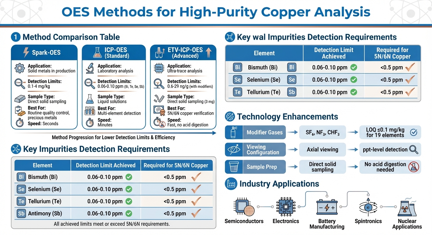
Optical Emission Spectroscopy (OES) is a highly effective method for detecting trace impurities in materials like high-purity copper. By exciting atoms to emit light, OES determines elemental composition with precision. Two main types are Spark-OES (used for solid metals in production) and ICP-OES (ideal for ultra-trace analysis in labs).
High-purity copper is crucial in industries like semiconductors and electronics, where even small impurities (e.g., bismuth, selenium, lead) can degrade performance. OES, particularly ETV-ICP-OES, enables accurate detection of these impurities at levels as low as 0.6 ng/g, ensuring quality control. Unlike other methods like XRF or AAS, OES analyzes bulk composition, provides multi-element detection, and delivers results quickly – often in seconds.
Modern advancements, such as halogenation modifiers and axial plasma viewing, have further improved sensitivity, enabling detection of impurities at sub-ppm levels. This makes OES indispensable for industries requiring precise material purity. Applications include quality control in electronics, spintronics, and battery manufacturing, where material integrity is critical.
OES Methods Comparison: Detection Limits and Applications for High-Purity Copper Analysis
Research Studies on Trace Impurity Detection in High-Purity Copper
ICP-OES with Axial Plasma Viewing for Copper Analysis
Inductively Coupled Plasma Optical Emission Spectroscopy (ICP-OES) with Electrothermal Vaporization (ETV) has proven effective for detecting trace impurities in high-purity copper. Using gaseous halogenation modifiers like CHF₃, SF₆, NF₃, and CF₄ allows trace elements to be separated from the copper matrix, preventing molten copper from overwhelming the plasma. This method achieves detection levels as low as 0.6–29 ng/g [1][2].
An oxidized copper surface enhances sensitivity during vaporization, improving the detection process [1]. Moreover, researchers have shown that calibration for most trace elements can be successfully conducted using liquid multi-element aqueous solutions instead of solid standards. This adjustment simplifies the analytical process without compromising accuracy [1].
High-Resolution OES for Sub-ppm Trace Elements
High-resolution Optical Emission Spectroscopy (OES) builds on these methods to refine impurity detection, especially for elements like bismuth (Bi), lead (Pb), selenium (Se), and tellurium (Te) at sub-ppm levels. While halogenation modifiers are effective for most elements, Se and Te require a different approach. Studies reveal that thermo-hydrogenation, which uses a hydrogen/argon (H₂/Ar) gas mixture as a modifier, significantly improves detection for these elements where halogenation alone falls short [2].
Using SF₆ and NF₃ modifiers, the limit of quantitation (LOQ) for 19 trace elements is typically ≤0.1 mg/kg. For Se and Te, the H₂/Ar modifier reduces LOQs even further, to below 0.1 mg/kg [2]. This is a significant advancement compared to older spectrographic methods from the 1970s, which were limited to detecting impurities at around 10 ppm [3]. Additionally, modern ETV-ICP OES techniques offer time and cost efficiency by enabling direct solid sampling and automation, making them ideal for routine quality control [1].
OES Applications in High-Purity Ceramics and Related Materials
Techniques initially developed for high-purity ceramics and platinum group metals (PGMs) have been adapted for copper analysis, addressing challenges such as the availability of reference materials. For example, research on ultra-pure PGMs demonstrates that spiking pure metal sponges with metal oxides and melting them in a vacuum induction furnace can produce reliable in-house calibration standards for OES [5]. This method has been effectively applied to copper analysis.
Spark-OES studies on high-purity precious metals have reported detection limits ranging from 0.1 mg/kg to 4 mg/kg for a broad spectrum of impurities [5]. Additionally, research across various high-purity metals like aluminum (Al), gallium (Ga), indium (In), and zinc (Zn) highlights the importance of managing matrix concentrations to minimize spectral interferences during ICP-OES analysis [6]. While high-resolution ICP-MS is often favored for ultra-trace analysis, ICP-OES remains essential for multi-element trace work when matrix effects are carefully controlled [6].
This content is for informational purposes only. Consult official regulations and qualified professionals before making sourcing or formulation decisions.
Common Technical Methods in OES Studies
Emission Line Selection and Spectral Interference Management
When performing trace analysis, selecting the right emission lines is critical for achieving precise results. Analysts rely on an atlas that highlights key emission lines for 70 elements to guide this process and minimize interference [7].
One effective method involves comparing spectral profiles of common matrix elements with those of the target analyte. This helps identify overlapping signals that could lead to inaccuracies. For instance, sodium (Na) emissions at 590 nm often interfere with iron oxide (FeO) spectral bands [8]. In October 2011, a team led by Jürgen Hassler from ESK Ceramics GmbH and the BAM Federal Institute for Materials Research and Testing demonstrated a practical solution. By using CHF₃ as a gaseous halogenation modifier, they achieved in situ separation of the analyte from the matrix. This approach reduced matrix interference in the plasma, enabling the detection of 20 trace elements with quantification limits between 0.6 ng/g and 29 ng/g [1].
Advanced digital processing techniques, such as the airPLS algorithm and MCR-ALS, further enhance the accuracy of spectral analysis. These methods effectively remove baseline noise and deconvolute overlapping signals. For example, researchers from the University of Concepción in Chile, including Gonzalo Reyes and Carlos Toro, applied these techniques in January 2021 to analyze copper oxide emissions during sulfide combustion. By using airPLS for noise removal and MCR-ALS for signal clarification, they identified distinct CuO peaks at 606 nm and 616 nm that were previously obscured [8].
"The extracted spectral pattern is directly correlated with the emission profile reported in the literature, evidencing the potential of using spectral analysis techniques on copper sulfide combustion spectra." – Reyes, G., et al. [8]
Another key factor in improving detection sensitivity is optimizing the plasma viewing configuration.
Plasma Viewing Configurations and Detection Limits
The way the plasma is viewed – either axially (end-on) or radially (side-on) – has a major impact on detection sensitivity. Axial viewing, for example, is ideal for detecting elements at extremely low levels, such as parts per trillion (ppt) [9].
In the analysis of high-purity copper, axial viewing allows for the detection of impurities like bismuth, tellurium, selenium, and antimony at concentrations as low as 0.06 to 0.100 ppm in solid copper matrices. In a 5% copper solution, it can detect these impurities in the single parts per billion (ppb) range [9]. However, achieving this level of sensitivity requires fine-tuning of operational parameters. Researchers Sergei Leikin and Autumn Phillips found that lower nebulizer flow rates and higher RF power settings are typically ideal for maximizing sensitivity [9].
On the other hand, radial viewing offers greater resilience against matrix interferences, making it better suited for samples with high total dissolved solids (TDS). While less sensitive than axial viewing, radial viewing is advantageous for handling samples with up to 10 times more TDS than ICP-MS can manage. Despite this, axial viewing remains the preferred choice for routine quality control of high-purity materials due to its superior detection capabilities.
The accuracy of these methods also depends heavily on proper sample preparation and matrix matching.
Sample Preparation and Matrix Matching
Accurate and reproducible OES results start with meticulous sample preparation. Techniques such as surface oxidation and the use of CHF₃ during electrothermal vaporization improve analyte release and separation. These methods reduce interference and eliminate the need for lengthy acid digestion processes [1].
Gaseous halogenating modifiers, like CHF₃, are particularly effective for separating analytes from complex matrices such as copper. Calibration for most trace elements can be performed using liquid multi-element aqueous solutions. However, elements like silver (Ag), magnesium (Mg), and nickel (Ni) often require matrix-matched solid standards to ensure accuracy [1].
"A sufficient in situ analyte matrix separation was achieved by using CHF₃ as halogenating reagent avoiding a high matrix input from the molten copper sample into the ETV system and the plasma." – Jürgen Hassler et al. [1]
Matrix matching plays a crucial role in ensuring that calibration standards closely mirror the sample composition. This step helps account for matrix effects that could otherwise distort the results. For high-purity materials, even slight differences in the matrix can significantly affect measurement precision. While halogenation is effective for most elements, specialized methods may be needed for elements like selenium (Se) and tellurium (Te), which are not easily released under standard ETV conditions.
This content is for informational purposes only. Consult official regulations and qualified professionals before making sourcing or formulation decisions.
Analytical Performance and Industry Applications
Detection Limits for Trace Impurities in Copper
Modern ICP-OES systems are capable of detecting impurities in 5N and 6N copper at incredibly low levels, as low as 0.5 ppm. For elements like Bismuth (Bi), Tellurium (Te), Selenium (Se), and Antimony (Sb), axial viewing achieves detection limits between 0.06 and 0.10 ppm. Additionally, other trace elements can be measured down to the parts-per-trillion (ppt) range [9]. Enhanced techniques like ETV-ICP-OES further improve detection limits without requiring acid digestion [1]. When paired with modifier gases such as SF₆ or NF₃, the limits of quantification (LOQs) for 19 trace elements drop to ≤0.1 mg/kg [2].
"To meet such high purity grade requirements [99.999% or 99.9999%], the impurities have to be analyzed at extremely low levels of 0.5 ppm in the solid material." – Sergei Leikin and Autumn Phillips [9]
| Impurity Element | ICP-OES Detection Limit (Solid Cu) | ETV-ICP-OES LOQ (Solid Cu) | Required for 5N/6N Copper |
|---|---|---|---|
| Bismuth (Bi) | 0.06–0.10 ppm [9] | < 0.1 mg/kg [2] | < 0.5 ppm [9] |
| Antimony (Sb) | 0.06–0.10 ppm [9] | < 0.1 mg/kg [2] | < 0.5 ppm [9] |
| Selenium (Se) | 0.06–0.10 ppm [9] | < 0.1 mg/kg [2] | < 0.5 ppm [9] |
| Tellurium (Te) | 0.06–0.10 ppm [9] | < 0.1 mg/kg [2] | < 0.5 ppm [9] |
This level of precision is critical because even the smallest impurities can negatively impact copper’s performance in demanding applications.
How Trace Impurities Affect Material Properties
The presence of trace impurities can have a significant impact on copper’s performance, altering its electrical, thermal, and structural characteristics. Homogeneity throughout the material is essential to ensure consistent properties across production batches. In a study conducted in June 2017 by Thomas Bacquart and Jürgen Hassler at the European Commission’s Joint Research Centre (JRC), ETV-ICP-OES was used to analyze homogeneity in electrolytic copper reference materials (ERM-EB074C and ERM-EB075C). This method provided greater precision compared to traditional acid dissolution, achieving relative standard deviations below 8% for most elements [10]. Additionally, the study demonstrated that the minimum sample size for elements like gold (Au), lead (Pb), selenium (Se), and tellurium (Te) could be reduced from 10 mg to smaller quantities without compromising accuracy [10].
"ETV-ICP-OES was more precise than digestion methods with relative standard deviations of less than 8% for most elements." – Thomas Bacquart, Joint Research Centre [10]
OES in Routine Quality Control
The advanced capabilities of OES directly support the stringent quality control processes required for high-purity materials. Direct solid sampling OES has become a cornerstone in regulated industries due to its ability to eliminate complex preparation steps like acid digestion. This not only reduces contamination risks but also saves time and costs [1][10]. Modern ETV-ICP-OES methods require as little as 3 mg of sample material, compared to the 10 mg needed for older digestion-based methods [10].
In March 2014, Anglo American Platinum adopted Spark-OES at its final metals laboratory to routinely analyze impurities – such as Au, Ag, Fe, Ni, and Cu – in refined platinum, palladium, and rhodium. Detection limits ranged from 0.1 mg/kg to 4 mg/kg, ensuring fast turnaround times for plant operations [5]. The near non-destructive nature of Spark-OES also helps preserve valuable materials during testing [5].
"The developed direct solid sampling method is time and cost effective and well suited for the characterization of high-purity copper materials." – Jürgen Hassler, ESK Ceramics GmbH & Co. KG [1]
These OES techniques are integral to real-time monitoring during production, ensuring that materials meet rigorous industry standards. This is particularly vital in regulated settings where batch consistency and traceability are non-negotiable.
This content is for informational purposes only. Consult official regulations and qualified professionals before making sourcing or formulation decisions.
sbb-itb-aa4586a
Future Developments in OES for High-Purity Material Analysis
OES Technology Advancements for Enhanced Sensitivity
Emerging OES systems are tackling the challenge of detecting trace impurities with some groundbreaking innovations. One example is the integration of Electrothermal Vaporization (ETV) with ICP-OES, which eliminates the need for acid digestion. This approach has proven especially useful for analyzing materials like silicon carbide and nuclear-grade graphite, where traditional wet chemical methods often fall short [4]. These advancements are simplifying analytical workflows significantly.
In 2016, researchers from BAM and SPECTRO Analytical Instruments introduced SF₆ and NF₃ modifiers for ETV-ICP-OES, achieving detection limits (LOQs) as low as ≤0.1 mg/kg for 19 elements in high-purity copper [2]. This method allowed calibration using aqueous solutions, streamlining the verification process. The modifiers help form volatile halides, making it possible to detect elements like titanium, zirconium, and vanadium, which are typically challenging to volatilize [2].
Modern spectrometers are also pushing the boundaries with high-resolution optics offering 5 pm bandwidth and solid-state imaging detectors. These advancements enable simultaneous multi-element analysis with real-time error correction [11][12]. Such improvements are particularly beneficial for on-site analysis, enhancing both speed and precision. As John W. Olesik, Research Scientist and Director of the Trace Element Research Laboratory at The Ohio State University, aptly noted:
"If we will have self-driving cars, why not intelligent (‘self-driving’) ICP-OES instruments that can identify and overcome potential errors without an expert instrument operator?" [12]
Impact on High-Purity Supply Chains
These technological strides are reshaping verification processes in regulated industries. The ability to conduct rapid, direct solid sampling via ETV-ICP-OES is especially crucial for sectors like semiconductors, electric vehicles, and nuclear applications, where even minute impurities can compromise material performance [4][12].
In March 2024, researchers from TU Bergakademie Freiberg and Sensmet Oy successfully employed micro-discharge optical emission spectroscopy (μDOES) for on-site analysis of lithium salt solutions. This system measured impurities such as Na, K, Al, Fe, and Zn in lithium carbonate and hydroxide solutions, achieving detection limits in the low μg/L range and a relative standard deviation of just 3% over 9 hours [13]. μDOES generates a micro-plasma directly within aqueous samples, eliminating the need for a carrier gas and enabling real-time monitoring of industrial processes in the battery metal supply chain [13].
By integrating real-time monitoring directly into production timelines, on-site OES methods are revolutionizing quality control. For companies like specialty chemical providers, these rapid analytical techniques ensure rigorous quality assurance and maintain supply chain reliability. For instance, Allan Chemical Corporation (https://allanchems.com), known for its sourcing-first approach, relies on such innovations to deliver high-purity materials essential for regulated industries. As demand for battery-grade lithium and ultra-pure copper continues to rise, these advancements are becoming indispensable for meeting industry standards.
This content is for informational purposes only. Consult official regulations and qualified professionals before making sourcing or formulation decisions.
Optical Emission Spectroscopy | Full Explanation & Precautions
FAQs
How does optical emission spectroscopy (OES) compare to other methods like X-ray fluorescence (XRF) or atomic absorption spectroscopy (AAS) for detecting impurities?
Optical Emission Spectroscopy (OES), including advanced methods like ICP-OES (Inductively Coupled Plasma OES) and ETV-ICP-OES (Electrothermal Vaporization ICP-OES), stands out as an effective tool for detecting trace impurities. One of its key strengths is the ability to analyze multiple elements simultaneously, with detection limits reaching as low as the parts-per-trillion (ppt) range. Beyond its precision, OES delivers results quickly – often in just minutes per sample. Solid-sampling techniques further enhance efficiency by cutting down preparation time, as they eliminate the need for lengthy acid digestion processes.
On the other hand, Atomic Absorption Spectroscopy (AAS) is more limited in scope. It typically measures one element at a time and has higher detection limits, usually ranging from parts-per-million (ppm) to sub-ppm levels. This makes AAS less practical for applications requiring multi-element analysis. While this section doesn’t include specific comparisons to X-ray Fluorescence (XRF), OES remains a highly efficient and precise option for analyzing trace impurities in high-purity materials like copper.
What are the advantages of using halogenation modifiers in optical emission spectroscopy (OES)?
Halogenation modifiers like CHF₃, SF₆, and NF₃ play a key role in Optical Emission Spectroscopy (OES). These compounds are introduced into the plasma or arc to transform trace elements into more volatile halide compounds. This transformation helps transport these elements more effectively into the excitation zone, leading to cleaner and more accurate emission signals.
Here’s why halogenation modifiers are valuable:
- Better detection of trace elements: Volatile halides improve the vaporization process, enabling the detection of elements such as chromium, titanium, and zirconium at extremely low concentrations.
- Minimized spectral interference: By isolating the analyte from the sample matrix, halogenation reduces interference from materials like copper, ensuring more accurate measurements.
- Increased efficiency: Stabilized arcs result in quicker, more consistent analyses and require minimal sample preparation.
Allan Chemical Corporation supplies high-purity halogenating reagents, specifically designed to support laboratories in achieving precise and dependable OES results.
Why is axial plasma viewing commonly used for detecting ultra-trace impurities?
Axial plasma viewing is a preferred method for detecting ultra-trace impurities because it captures light along the entire length of the plasma column. This extended optical path amplifies the signal intensity, allowing for higher sensitivity and lower detection limits compared to radial viewing.
By collecting more emitted light, axial viewing provides precise and dependable detection of even the tiniest impurities, making it ideal for analyzing high-purity materials such as copper.


Comments are closed