Sputtering targets are critical for Physical Vapor Deposition (PVD), a process used to create thin films on surfaces like silicon wafers or smartphone screens. These targets act as the material source, releasing atoms when struck by ionized gas in a vacuum chamber. The quality of the resulting films depends on the target’s composition, purity, and density, which directly affect performance in applications like semiconductors, optics, and solar panels.
Key facts:
- Purity: Semiconductor applications demand ultra-high purity, often ≥99.999% (5N), to prevent defects.
- Density: Targets must exceed 98% density to avoid trapped gases and ensure smooth films.
- Materials: Common options include metals (e.g., Aluminum, Copper), alloys (e.g., Titanium-Tungsten), and compounds (e.g., Indium Tin Oxide for transparent conductive layers).
Applications span from microchips and touchscreens to solar cells and medical coatings, where precision and uniformity are paramount. Selecting the right target involves evaluating material properties, manufacturing methods like Hot Isostatic Pressing (HIP), and supplier reliability to meet specific requirements.
This guide unpacks the sputtering process, material choices, and industry uses, offering practical insights for achieving high-quality thin films.
What Are Sputtering Targets?
A sputtering target is a solid material used in Physical Vapor Deposition (PVD) processes to create thin films. In PVD, the target acts as a cathode within a vacuum chamber, attracting positively charged ions – typically from an ionized inert gas like argon. When these high-energy ions collide with the target, they dislodge atoms, which then condense onto a substrate to form a thin film. This process highlights how the target’s physical and material properties influence the final film’s quality.
The target’s composition determines the characteristics of the deposited film. For example, aluminum targets yield aluminum films commonly used for conductive interconnects in microchips, while Indium Tin Oxide (ITO) targets are used to create transparent conductive layers for devices like touchscreens. Targets come in various shapes, with planar and rotatable (cylindrical) designs being the most common. Planar targets are often used in research and development, while rotatable targets, which spin during operation to ensure even wear, are favored in high-volume manufacturing.
Physical properties play a critical role in performance. For applications in semiconductors and optics, targets must have a density exceeding 98% to minimize defects in the thin film. Purity levels also vary depending on the application, ranging from 99% (2N) for general industrial uses to 99.9999% (6N) for ultra-sensitive electronics. Additionally, smaller grain sizes improve sputtering rates and film uniformity, while high thermal conductivity helps dissipate heat generated during ion bombardment, preventing damage to the target. These factors are vital for producing high-quality films, especially in demanding industries like semiconductor manufacturing.
Sputtering targets are made from a broad range of materials, including pure metals (e.g., copper, titanium), alloys (e.g., titanium-tungsten), and ceramics (e.g., aluminum oxide). The choice of material depends on the application. Conductive metal targets are typically used with DC sputtering, while non-conductive ceramic targets require RF sputtering to avoid charge buildup.
This overview lays the groundwork for understanding how sputtering targets function within the PVD process.
This content is for informational purposes only. Consult official regulations and qualified professionals before making sourcing or formulation decisions.
sbb-itb-aa4586a
How Sputtering Targets Work in PVD
How PVD Sputtering Process Works: Step-by-Step Visualization
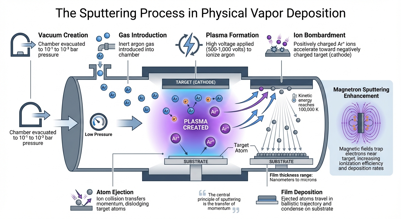
The Sputtering Process
To begin, the sputtering chamber is evacuated to a pressure between 10⁻¹ and 10⁻³ bar, after which inert argon gas is introduced [8]. A high voltage, typically ranging from 500 to 1,000 volts, is then applied to ionize the argon gas. This electrical field strips electrons from the argon atoms, creating a plasma composed of positively charged ions (Ar⁺) and free electrons. The sputtering target, which acts as the negatively charged cathode, attracts these ions. When the ions collide with the target, they transfer momentum, dislodging atoms from its surface.
"The central principle of sputtering is the transfer of momentum." – Kintek Solution [7]
These ejected atoms travel through the vacuum in a ballistic trajectory and condense on the substrate, forming thin films. Depending on the application, these films can range from nanometers to microns in thickness [4]. This process not only enables atomic-level film formation but also ensures excellent adhesion and uniformity, leading to reliable and consistent results.
Benefits of Sputtering in PVD
Sputtering stands out as a preferred method for creating high-performance thin films due to several key advantages. The high kinetic energy of the sputtered atoms – reaching temperatures as high as 100,000 K – results in dense films that adhere strongly to the substrate [10]. This strong adhesion makes the films resistant to peeling or delamination, even under mechanical or thermal stress.
The process’s atomic-level precision allows for exceptional control over film thickness and uniformity. Because the film builds layer by layer, manufacturers can meet exact specifications down to the nanometer scale. This level of precision is particularly important in semiconductor manufacturing, where even slight variations in thickness can impact device performance. Additionally, the high-purity vacuum environment reduces the risk of contaminants, ensuring the integrity of the final film.
Magnetron sputtering further enhances the process by using magnetic fields to trap electrons near the target surface. This increases ionization efficiency and deposition rates [8]. As a result, manufacturers can achieve faster production cycles and operate at lower pressures without compromising film quality. Magnetron sputtering also supports reactive sputtering, where gases like oxygen or nitrogen are introduced to form compound films – such as oxides or nitrides – directly from metal targets [9]. For instance, a titanium target can produce pure titanium films using DC sputtering or titanium nitride coatings when nitrogen gas is added.
This content is for informational purposes only. Consult official regulations and qualified professionals before making sourcing or formulation decisions.
Materials Used for Sputtering Targets
Sputtering targets are generally divided into three main groups: pure metals, alloys, and ceramics (which include oxides, nitrides, and carbides) [2][1]. Each type is selected based on the specific properties it offers, which influence the composition, purity, and performance of the resulting thin films.
Metals and Alloys
The choice of material for sputtering targets plays a critical role in determining the functional performance of the deposited films. Pure metal targets are highly favored in semiconductor and electronics manufacturing because of their excellent electrical and thermal conductivity. Commonly used metals include Aluminum (Al), Copper (Cu), Titanium (Ti), and Gold (Au), all of which are integral to Physical Vapor Deposition (PVD) processes [2][1]. These metals are chosen for their unique conductivity properties, which directly enhance the efficiency and reliability of the films. For instance, Titanium and Tantalum (Ta) are often applied as barrier layers in semiconductor production [3].
Alloy targets, on the other hand, are created by combining two or more metals to achieve desired properties that pure metals cannot provide. For example, Nickel-Chromium (NiCr) is widely used in thin-film resistors due to its stable resistance and low sensitivity to temperature changes [11]. Similarly, Titanium-Tungsten (TiW) improves film adhesion and acts as a diffusion barrier, preventing unwanted interactions between metal interconnects and silicon substrates [2]. These tailored compositions allow manufacturers to optimize properties such as electromagnetic behavior, corrosion resistance, and mechanical durability, making them ideal for applications like magnetic data storage and decorative coatings [6].
Oxides and Compounds
Ceramic and compound targets expand the range of materials available for sputtering, offering benefits like chemical stability, high melting points, and specific optical or electrical characteristics. Indium Tin Oxide (ITO) is a prime example, as it combines electrical conductivity with optical transparency, making it essential for LCDs and touchscreens [2][6]. Zinc Oxide (ZnO) serves similar purposes in solar panels and display technologies, while Aluminum Oxide (Al₂O₃) is valued for its insulating and corrosion-resistant properties in protective layers [2].
In addition to oxides, compound targets include materials like Cadmium Sulfide (CdS), which is used in the absorber layers of thin-film photovoltaic cells [2][11]. Titanium Nitride (TiN) is another notable compound, offering a gold-like appearance and exceptional wear resistance, making it suitable for decorative finishes and cutting tools [2]. Magnesium Fluoride (MgF₂) is commonly used in optical coatings due to its transparency across ultraviolet and infrared wavelengths [2]. These specialized compounds enable the deposition of films with unique characteristics – such as enhanced hardness, transparency, or semiconductivity – that cannot be achieved with pure metals alone. This wide selection of materials ensures that sputtering targets can meet the specific needs of various industries.
This content is intended for informational purposes only. Always consult official guidelines and qualified experts before making sourcing or formulation decisions.
Where Sputtering Targets Are Used
Sputtering targets play a crucial role in enabling ultra-thin film deposition, driving advancements across industries like microchips, solar panels, and more. Here’s how they contribute to key applications:
Semiconductor and Electronics
Sputtering targets are indispensable in the production of semiconductors and electronic devices. In semiconductor manufacturing, they are used to deposit thin layers of metals and dielectrics onto silicon wafers. These layers form conductive interconnects and barrier layers, which prevent material diffusion and ensure stable electrical performance [2]. For advanced nodes below 110 nm, materials like copper and tantalum are preferred for their low resistance, while aluminum and titanium are commonly used for larger nodes [3]. These applications require ultra-high purity levels, often reaching 99.999% (5N) or more [2].
Flat-panel displays depend on sputtered transparent conductors like indium tin oxide (ITO), while data storage devices use sputtered magnetic thin films, frequently made from cobalt-based alloys, to support high-density storage [2].
Optical and Protective Coatings
Sputtering targets are vital in creating optical coatings for applications like anti-reflective (AR) layers, filters, and mirrors used in cameras, lenses, and precision instruments. Materials such as silicon dioxide (SiO₂), titanium dioxide (TiO₂), and magnesium fluoride (MgF₂) are deposited to optimize light reflection and transmission, enhancing clarity and performance [2].
For protective purposes, sputtered coatings improve hardness, wear resistance, and corrosion resistance. Titanium nitride (TiN) and diamond-like carbon (DLC) coatings are applied to cutting tools, automotive parts, and consumer goods, extending their durability and lifespan [2]. In the medical field, sputtering is used to apply biocompatible coatings on devices like orthopedic implants, dental tools, and surgical instruments, offering better adhesion and uniformity compared to other methods [4].
Sputtering also supports energy solutions by forming efficient photovoltaic and thermoelectric layers, contributing to advancements in renewable energy technologies.
Solar and Energy Industries
In the solar industry, sputtering targets are essential for producing thin-film photovoltaic (PV) layers that convert sunlight into electricity. Materials like copper indium gallium selenide (CIGS) and cadmium telluride (CdTe) are used for absorber layers, while zinc oxide (ZnO) and indium tin oxide (ITO) serve as transparent conductive oxides (TCOs), allowing light to pass through while maintaining electrical conductivity [2]. Molybdenum (Mo) is another key material, used for back contacts and electrodes due to its excellent conductivity and adhesion properties [4].
Sputtering is particularly valued in large-scale solar panel production because it provides uniform coatings over extensive glass surfaces. Additionally, cylindrical (rotatable) targets are gaining popularity in solar manufacturing for their higher material efficiency and consistent coatings across large areas [4]. Beyond solar panels, materials like bismuth telluride (Bi₂Te₃) are utilized in thermoelectric generators to enhance energy efficiency [2].
This content is for informational purposes only. Always consult official guidelines and qualified experts before making sourcing or formulation decisions.
How to Select Sputtering Targets
Choosing the right sputtering target is key to achieving the precise thin-film characteristics outlined in this guide. This decision requires careful evaluation of material properties, manufacturing practices, and supplier reliability to meet your specific Physical Vapor Deposition (PVD) needs.
Material Purity and Consistency
Purity directly impacts the performance and durability of your thin films. As Julissa Green, a Chemistry Specialist at Stanford Advanced Materials, explains:
"Thin-film coatings live or die depending on purity" [2].
Impurities can lead to particle formation, which weakens adhesion, accelerates peeling, and disrupts electrical performance. Standard coatings typically require 99.9% purity, but more demanding applications like semiconductor processes call for higher levels – ranging from 99.995% to 99.9999% purity. For instance, 0.35μm integrated circuits need at least 99.995% purity, while advanced 0.18μm applications demand 5N (99.999%) to 6N (99.9999%) purity [13]. Optical coatings and magnetic films also benefit from purities of 99.995% or higher to avoid absorption defects and maintain clarity [2].
High-density targets – achieving over 98% density for cast materials and 97% for powder-metallurgy products – are essential for smoother films, better thermal stability, and enhanced sputtering rates. These targets also ensure consistent film thickness [5][13]. Low-density targets, on the other hand, may contain pores that trap oxygen and water vapor, leading to contamination, cracking, and poor adhesion during deposition. Once the material metrics are verified, it’s crucial to ensure your supplier adheres to strict quality standards.
Supplier Certifications and Quality Standards
Supplier reliability plays an equally important role in ensuring sputtering target performance. Certified suppliers reduce contamination risks and guarantee consistent quality. Look for manufacturers that follow recognized quality management systems and utilize advanced testing methods like X-ray fluorescence (XRF), inductively coupled plasma (ICP) analysis, and ultrasonic testing to confirm the required purity and density levels for your application [2].
Advanced manufacturing processes such as Hot Isostatic Pressing (HIP) and Cold Isostatic Pressing (CIP) are valuable for increasing target density and minimizing internal voids. These techniques help maintain stable sputtering rates and reduce the risk of film defects [5]. Additionally, certified suppliers often use protective measures like vacuum-sealed packaging or nitrogen purges for reactive metals (e.g., copper, aluminum) to prevent oxidation during transport and storage. When assessing suppliers, request documentation of their testing and handling protocols to ensure they meet your specific purity and density standards.
This content is for informational purposes only. Consult official regulations and qualified professionals before making sourcing or formulation decisions.
Conclusion
Sputtering targets play a key role in achieving precise thin-film deposition through Physical Vapor Deposition (PVD). These carefully crafted materials are essential for producing uniform, high-quality coatings used in semiconductors, optics, solar panels, and protective layers. The sputtering process itself – where energized ions bombard the target to release atoms that coat a substrate – relies on strict material standards to ensure consistent performance.
Whether made from pure metals, specialized alloys, or oxide compounds, each application has specific requirements for purity and density. For instance, semiconductor applications demand ultra-high purity materials, while optical coatings and magnetic films often require densities above 98% to maintain film integrity and prevent defects[2].
Targets with high density and uniform grain structures produce smoother, more stable films, while lower-quality targets can lead to contamination, arcing, and early failure. With the global semiconductor sputtering target market expected to grow at an annual rate of 5.6% through 2030[12], advanced manufacturing techniques like Hot Isostatic Pressing (HIP) are becoming increasingly important to meet the density demands of modern electronics[5].
Reliable suppliers are essential to this process. Those who employ rigorous testing methods, such as X-ray fluorescence (XRF) and inductively coupled plasma (ICP) analysis, along with strict handling measures like vacuum-sealed packaging and regular inspections, help ensure materials meet the required standards. These practices underscore the importance of sputtering targets in enabling high-performance coatings across a wide range of industries.
This content is for informational purposes only. Always consult official regulations and qualified professionals for sourcing or formulation decisions.
FAQs
How do I choose between planar and rotatable targets?
The right option depends on what you’re producing and how much you need. Planar targets work best for small-scale projects, prototypes, or applications that demand precise coatings. However, they aren’t the most economical choice for large-scale manufacturing. On the other hand, rotatable targets are suited for continuous sputtering over large areas. They provide longer runtimes, better material usage (up to 80%), and are more cost-effective for high-volume production. Your decision should align with your production scale and efficiency goals.
What purity level do I need for my application?
The purity level of sputtering targets is determined by the demands of your specific application. For high-precision fields like semiconductor manufacturing, metals with a purity of 99.99% or higher are often required to minimize contamination and ensure consistent results. On the other hand, applications with less stringent requirements may find 99.9% purity adequate. While higher purity targets provide cleaner and more uniform coatings, they also come with a higher price tag. It’s important to balance purity with your process requirements and consult your supplier for tailored advice.
When should I use DC vs RF sputtering?
DC sputtering is a great choice for electrically conductive targets like metals. It stands out for its straightforward process and lower costs. On the flip side, RF sputtering excels with insulating or semi-insulating materials, such as oxides (e.g., SiO₂). It also delivers smoother films with improved packing density. Use DC sputtering for efficiency when handling conductive materials, and opt for RF sputtering when film quality or non-conductive targets are the priority.


Comments are closed