Material compatibility in Physical Vapor Deposition (PVD) is key to ensuring reliable semiconductor performance. This process involves depositing thin films of materials like Aluminum, Copper, Titanium, Gold, TiAl (Titanium Aluminum), NiCr (Nickel Chromium), Silicon Nitride, and Chromium Nitride onto substrates under high-vacuum conditions. Each material contributes unique properties that impact electrical conductivity, thermal stability, and adhesion, all of which are critical for applications like interconnects, barrier layers, and protective coatings.
Here’s a quick overview of the materials:
- Aluminum: Excellent conductivity; used in bond pads and metallization layers. Requires barrier layers to prevent diffusion.
- Copper: Superior conductivity; essential for advanced interconnects. Needs barrier layers due to diffusion risks.
- Titanium: Strong adhesion and thermal stability; used in barrier layers and as an adhesion promoter.
- Gold: Oxidation-resistant and highly conductive; reserved for specialty contacts and wire bonding.
- TiAl: Combines titanium’s stability with aluminum’s conductivity; ideal for high-temperature applications.
- NiCr: High resistivity; perfect for thin-film resistors and thermocouples.
- Silicon Nitride: Acts as a dielectric and diffusion barrier; provides insulation and device protection.
- Chromium Nitride: Conductive ceramic; offers corrosion resistance and mechanical durability.
The choice of material depends on factors like thermal expansion, film adhesion, and electrical performance. For example, Copper’s low resistivity enables faster devices, but it requires robust barrier layers to prevent diffusion. Similarly, Titanium’s adhesion properties make it indispensable for creating reliable interfaces between layers. Each material’s unique characteristics must align with the specific demands of the semiconductor application.
This article dives into the properties, challenges, and applications of these materials, providing insights into their roles in modern semiconductor manufacturing.
S9.1 Deposition Technologies in Semiconductor Equipment Manufacturing: Tools, Techniques, Trend
1. Aluminum
Aluminum plays a central role in semiconductor PVD processes, particularly in slab metallization, bondpad creation, and as a fill-in metal for various layers. Its popularity stems from its excellent conductivity, low resistivity, and the natural formation of a corrosion-resistant oxide layer [10][11]. These properties make it a reliable choice for ultra-thin, high-purity film deposition in the industry.
Purity Levels
The effectiveness of aluminum largely depends on its purity. Advanced semiconductor technologies, such as 28-nanometer HKMG (High-K Metal Gate) nodes, require ultra-pure aluminum to maintain high conductivity and ensure superior film quality. In some cases, aluminum alloys like Al-Cu, Al-Ta, or Al-Nd are used to enhance resistance to electromigration and minimize hillock formation during thermal processing [10][11][12][13].
Thermal and Chemical Stability
Deposition temperatures ranging from 320°F to 800°F (160°C to 427°C) significantly impact aluminum’s resistivity and grain structure. Two-step Cold-Hot deposition processes are preferred for achieving lower resistivity and finer grain sizes compared to single-step methods [13][14]. However, interactions between aluminum and titanium wetting layers, which can form TiAl₃, may complicate subsequent CMP (Chemical Mechanical Planarization) steps [13].
Thermal stability is critical, but aluminum’s electrical performance is equally important in ensuring its reliability in semiconductor applications.
Electrical Conductivity
Aluminum’s electrical properties are a major reason for its widespread use in PVD processes. It is the preferred material for top fill-in metal layers in Replacement Metal Gate structures due to its lower resistance compared to tungsten [13]. However, high current densities can lead to electromigration, which poses a risk of device failure [1][2]. Process optimization is crucial: CHAL films (Cold-Hot Aluminum Layers) demonstrate more stable resistivity across different wetting layer thicknesses than HAL (Hot Aluminum Layers) films. For 28-nanometer nodes, titanium wetting layers thicker than 40 Å are necessary to meet gapfill and planarization requirements [13].
PVD Process Suitability
Aluminum deposition under ultra-high vacuum conditions (10⁻² to 10⁻⁶ Torr) ensures excellent step coverage. Systems operating at 392°F (200°C) under these conditions can achieve similar results to those running at 572°F (300°C) in standard setups [1][9]. Additionally, barrier layers like titanium or titanium nitride are essential to prevent aluminum diffusion into silicon substrates. This makes aluminum an ideal choice for applications requiring precise layer control and moderate conductivity [1][2].
By combining material-specific strategies with precise process control, aluminum continues to deliver reliable performance in semiconductor PVD processes.
This content is for informational purposes only. Consult official regulations and qualified professionals before making sourcing or formulation decisions.
2. Copper
Copper is a cornerstone material for interconnects, thanks to its excellent conductivity and resistance to electromigration. With an electrical resistivity of just 1.7 μΩ·cm – far lower than aluminum’s 2.65 μΩ·cm – copper allows for the design of smaller, faster, and more energy-efficient devices [18]. However, achieving these advantages hinges on maintaining strict purity standards.
Purity Levels
Copper sputtering targets can reach purity levels as high as 6N (99.9999%), which is crucial for preserving the electrical properties of deposited films [16]. High purity impacts the crystal structure and grain size, with larger grains reducing electrical resistance and enhancing device performance [17]. That said, impurities, such as argon from the sputtering gas, can still be introduced during deposition [4]. In ionized PVD (Physical Vapor Deposition) systems using radio frequency generators, up to 95% of copper atoms can be ionized, which improves deposition in high-aspect-ratio structures [18]. This level of purity ensures consistent and reliable deposition in advanced PVD processes.
Thermal and Chemical Stability
While purity is essential, copper’s thermal and chemical stability also play a critical role. Copper tends to diffuse quickly into silicon and silicon dioxide, which can cause severe device degradation or even failure [2][18]. To counter this, barrier layers – typically made of materials like titanium, titanium nitride, tantalum, or silicon nitride – are deposited via PVD before the copper layer [1][2]. Copper PVD processes operate at temperatures ranging from 50°C (122°F) to 500°C (932°F), making them suitable for heat-sensitive substrates while maintaining high film purity [1][15]. Additionally, copper’s resistance to electromigration significantly extends the operational life of semiconductor interconnects [1][2].
Electrical Conductivity
Copper’s exceptional electrical conductivity is a primary reason for its dominance in semiconductor PVD applications. It is the go-to material for creating low-resistance interconnects and conductive pathways, which enhance signal transmission and improve device reliability [1][2]. PVD processes achieve a sticking coefficient of 0.7–0.8 [17]. Advanced hollow cathode magnetron sources can further optimize copper deposition by generating plasma densities exceeding 10¹³ cm⁻³, offering precise control over the process [18].
PVD Process Suitability
In semiconductor manufacturing, PVD is primarily used to deposit thin copper seed layers, which are essential for subsequent Electrochemical Deposition (ECD) to fill trenches and vias [17][18]. Copper works well with both DC sputtering and E-beam evaporation, with E-beam evaporation producing particularly high-purity films [19][10]. While traditional magnetron sputtering can struggle with narrow trenches – sometimes leading to voids – ionized PVD methods provide superior bottom coverage in sub-250 nm structures [18]. The industry has also adopted Damascene processing, where trenches etched into dielectrics are filled with copper. This shift occurred because copper is challenging to etch using reactive ion etching below 150°C (302°F) [18]. Moreover, PVD processes are conducted in high-vacuum environments (10⁻² to 10⁻⁶ Torr) to minimize contamination [1].
This content is for informational purposes only. Consult official regulations and qualified professionals before making sourcing or formulation decisions.
3. Titanium
Titanium’s unique properties make it an essential material in advanced semiconductor applications. Its role as an adhesion promoter and diffusion barrier in Physical Vapor Deposition (PVD) processes is particularly noteworthy. Titanium’s high oxygen affinity allows it to scavenge residual moisture and form strong oxide bonds with dielectric layers, ensuring reliable adhesion between layers – an essential factor for maintaining device integrity. Additionally, titanium is often used in the form of titanium nitride (TiN), a compound with an exceptionally high melting point of 2,950°C (5,342°F) [8][27].
Purity Levels
The purity of titanium targets is critical for achieving optimal deposition results. Targets with purity levels ranging from 99.99% to 99.9995% are preferred, as lower-purity grades (e.g., 99.7%) can lead to the formation of convex particles that risk causing defects in circuits [21][23][24]. For instance, a titanium target with 99.999% purity achieves a deposition rate of 16.3 nm/min, while lower-purity targets often deposit at slower rates [24]. Oxygen contamination is a particular concern, as it can make titanium brittle and increase film resistivity, impairing carrier migration [22][24]. Furthermore, titanium with equiaxed α-phase grains offers better sputtering performance compared to grains with twin boundaries or β-phase structures [24].
In addition to purity, titanium’s behavior under thermal and chemical stresses plays a significant role in its effectiveness during PVD processes.
Thermal and Chemical Stability
Titanium’s performance in high-energy Ionized Metal Plasma (IMP) processes can be affected by its interaction with underlying materials. For example, it may react with aluminum to form resistive TiAlₓ compounds [25]. To mitigate this, manufacturers often use a hybrid deposition approach, starting with a thin titanium layer deposited in a non-ionized mode before switching to high-energy IMP deposition [25]. Another challenge is the thermal expansion mismatch between titanium (9.3 ppm/K) and silicon (2.3 ppm/K), which can cause stress in films at elevated temperatures, potentially affecting adhesion if the films are too thick [27]. Despite these challenges, titanium exhibits excellent corrosion resistance due to a passive oxide surface film and remains stable in steam up to approximately 400°C (752°F) [22].
These characteristics make titanium a reliable choice for precise PVD applications, even under demanding conditions.
Electrical Conductivity
Titanium’s electrical properties are another factor contributing to its widespread use. Bulk titanium has an electrical resistivity of 43 μΩ·cm, while PVD-deposited titanium films (100 nm thick) exhibit slightly higher resistivity at around 60 μΩ·cm [28]. Titanium nitride (TiN) films deposited via PVD offer lower resistivity (30–100 μΩ·cm) compared to Chemical Vapor Deposition (CVD) TiN films, which range from 200 to 10,000 μΩ·cm [26][27]. Purity directly influences resistivity; for example, films made from 99.999% purity titanium have a resistivity of approximately 6.9 × 10⁻⁶ Ω·m, while those from 99.7% purity measure around 9.8 × 10⁻⁶ Ω·m [24]. Additionally, surface roughness improves with higher purity, decreasing from 170 nm at 99.7% purity to 121 nm at 99.999% purity [24].
PVD Process Suitability
Titanium is commonly evaporated or DC sputtered in vacuum to create semiconductor barrier layers and improve adhesion. Advanced techniques like Ionized Physical Vapor Deposition (IPVD) and IMP enhance step coverage, achieving approximately 50% step coverage and over 40% bottom coverage in high-aspect-ratio features [20][25][28]. When depositing titanium nitride, PVD processes typically maintain a nitrogen-to-titanium ratio of 1:1, with oxygen contamination kept below 5 atomic percent [26]. Before titanium PVD begins, a degas step using infrared illumination is often performed to remove water from organic dielectrics. This is followed by a mild argon plasma sputter cleaning step to eliminate native oxides from metal surfaces [8].
This content is for informational purposes only. Consult official regulations and qualified professionals before making sourcing or formulation decisions.
4. Gold
Gold serves a specialized function in semiconductor PVD (Physical Vapor Deposition) processes due to its excellent electrical conductivity and resistance to oxidation. It is primarily used in wire bonding and ohmic contacts, making it a go-to material for applications where high reliability is essential[1][2]. Unlike other interconnect metals commonly used in the industry, gold is reserved for scenarios that demand unparalleled conduction stability.
Purity Levels
Maintaining the purity of gold is crucial in PVD processes. High-quality gold targets are used to produce pure, uniform films, which are essential for ensuring optimal device performance[2][10]. Any impurities in the target material can transfer directly into the thin film, potentially compromising its functionality. This makes the use of premium-grade targets a non-negotiable factor in achieving reliable results.
Thermal and Chemical Stability
Gold stands out for its exceptional chemical stability, with an oxidation potential of +1.50 V. This is significantly higher than metals like aluminum (–1.66 V), titanium (–1.63 V), and copper (+0.34 V)[8]. Its high oxidation potential prevents the formation of resistive oxide layers, ensuring long-term performance. However, gold can diffuse into certain metals, such as aluminum, which necessitates the use of barrier layers like titanium-tungsten (TiW) or nickel to maintain device stability. In gold bumping applications:
TiW acts as the adhesion, barrier, and UBM (Under Bump Metallization) metal, although, unlike in solder UBMs, the gold doesn’t form intermetallic phases with the TiW.[8]
Electrical Conductivity
Gold’s ability to maintain superior electrical conductivity over time makes it ideal for low-current or high-reliability electrical contacts. Materion highlights its advantages:
This metal makes a soft, inert, low-friction, high conductivity coating. As an electrical contact, it has exceptional corrosion resistance.[29]
Because gold does not form resistive oxides, its conductivity remains stable even in challenging environments. This reliability is critical in applications where oxidation must be minimized. For example, a typical PVD film stack for gold bumping includes a TiW layer (3,000 Å) for adhesion and diffusion barrier purposes, followed by a gold layer (1,000 Å)[8]. These PVD films, often thicker than electroplated layers, provide enhanced durability and long-term performance.
PVD Process Suitability
Gold deposition in PVD processes employs specialized techniques to address its adhesion challenges. Methods like vacuum evaporation, sputtering, and ion plating are used at controlled temperatures ranging from 50°C to 500°C[1][14][29][30]. Adhesion layers, such as titanium, nickel, or tantalum, are often required to ensure proper bonding to the substrate[1][29]. Additionally, evaporated gold tends to be softer than electroplated gold, which can be advantageous in applications requiring low friction and high conformability. Interestingly, the tensile stress of the gold seed layer can help balance the compressive stress of underlying barrier layers like TiW, contributing to the overall stability of the film[8].
This content is for informational purposes only. Always consult official regulations and qualified professionals before making sourcing or formulation decisions.
5. TiAl (Titanium Aluminum)
TiAl alloys bring noteworthy benefits to demanding processing environments, particularly in semiconductor PVD (Physical Vapor Deposition) applications. These alloys are prized for their high-temperature stability and exceptional resistance to oxidation. TiAl-based coatings, such as (Ti,Al)N, create a protective alumina layer that far surpasses the performance of standard titanium nitride in extreme conditions. This makes them ideal for applications where films must endure intense heat without breaking down. However, achieving these benefits requires strict control over purity and deposition parameters.
Purity Levels
The high-temperature capabilities of TiAl films hinge on maintaining exceptional material purity. Ultra-pure TiAl films are critical, and high-vacuum PVD systems (operating at 1×10⁻⁶–1×10⁻⁹ Torr) are essential to prevent contamination during deposition [33]. For reference, commercial titanium nitride sputtering targets – often used as a baseline for TiAl systems – are produced with 99.5% purity levels [31]. Even minor impurities during deposition can alter film properties like density, stress, and grain size, which can negatively impact etching and lithography performance, particularly in sub-0.25 μm features [32].
Thermal and Chemical Stability
One of TiAl’s standout qualities is its ability to thrive in high-temperature environments, thanks to its alumina-forming properties. Research in Surface and Coatings Technology highlights this advantage:
Because of their alumina-forming properties, (Ti,Al)N deposits show outstanding performance with respect to oxidation resistance and corrosion resistance by molten metals. [35]
The ternary compound Ti₃AlN demonstrates strong thermal stability, melting incongruently at approximately 1,863 K (about 2,894°F) [34]. However, during IMP (Ionized Metal Plasma) deposition, high-energy titanium ions can react with aluminum under-layers, forming resistive TiAlₓ compounds. This reaction can increase via resistance in deep-submicron devices [25]. To counteract this, a hybrid process is recommended: first deposit a thin titanium buffer layer in non-ionized mode before proceeding with IMP deposition [25].
PVD Process Suitability
Sputter deposition is a preferred method for producing TiAl alloy films, as it removes surface atomic layers while preserving the target’s composition [36]. This approach avoids the composition shifts that can occur with thermal evaporation, where differing vapor pressures lead to uneven enrichment of source materials. Ionized PVD techniques further enhance deposition, achieving over 40% bottom film coverage in 0.18-micron holes with aspect ratios as high as 8:1 [25]. Incorporating aluminum into titanium nitride improves grain refinement and microhardness, resulting in denser films with enhanced mechanical and chemical stability [35].
This content is for informational purposes only. Always consult official regulations and qualified professionals before making sourcing or formulation decisions.
sbb-itb-aa4586a
6. NiCr (Nickel Chromium)
NiCr alloys are crafted with precision to provide reliable resistance control, making them ideal for high-precision resistive layers in semiconductor PVD applications. Unlike traditional conductive metals, these alloys aren’t used for interconnects but excel in roles requiring stable resistance. The standard composition – 80% nickel and 20% chromium by mass – ensures low noise, efficient power dissipation, and a nearly zero temperature coefficient of resistance (TCR). These properties make NiCr a go-to material for integrated circuit resistors and thin-film thermocouples[37]. With an electrical resistivity of around 1.12 μΩ·m – roughly 66 times higher than that of copper – NiCr is perfect for applications demanding precise resistance control[38]. Below, we explore its purity, stability, and deposition characteristics.
Purity Levels
Semiconductor-grade NiCr sputtering targets must meet a minimum purity level of 99.9%. Specific impurities, such as nitrogen, aluminum, oxygen, silicon, and molybdenum, can be deliberately introduced to adjust sheet resistance and TCR. However, any unintended contamination during deposition in vacuum environments can significantly impair performance[1][37].
Thermal and Chemical Stability
NiCr naturally forms a protective 2 nm Cr₂O₃ layer, which prevents further oxidation and enhances its durability[39]. This layer remains stable even at NiCr’s high melting point of about 1,400°C (2,550°F), allowing it to withstand extreme temperatures[38]. In semiconductor applications, NiCr also serves as an adhesion promoter and diffusion barrier, effectively preventing base metal migration and intermetallic compound formation[29]. Additionally, thermal annealing can alter its microstructure – such as promoting crystallite growth – which impacts both resistivity and TCR. Rapid thermal processing, for instance, often reduces resistivity while increasing TCR[37].
PVD Process Suitability
Sputtering is the most effective PVD method for depositing NiCr films, as it ensures precise transfer of the alloy’s composition from the target to the film. Thermal evaporation, in contrast, risks altering the composition due to the different vapor pressures of nickel and chromium[36][39]. Sputtered NiCr films adhere strongly to substrates like glass, silicon wafers, and GaAs, thanks to the high kinetic energy of the sputtered atoms[39]. This method’s reliability and precise composition control make it the preferred choice for manufacturing thin-film resistors and strain gauges in microelectronics[39].
This content is for informational purposes only. Always consult official regulations and qualified professionals before making sourcing or formulation decisions.
7. Silicon Nitride
Silicon nitride (Si₃N₄) stands out from conductive metals and alloys used in semiconductor PVD due to its role as a dielectric material. Known for its insulating properties, chemical stability, and thermal resilience, it plays a critical role in semiconductor manufacturing. Unlike aluminum or copper, which conduct electricity, silicon nitride serves as a passivation layer and etch stop, offering protection against moisture, contaminants, and electrical interference. With a wide bandgap of about 5.2 eV and high electrical resistivity, it is a key material for safeguarding sensitive device structures [45]. Below, we’ll explore its purity, thermal behavior, and suitability for PVD processes.
Purity Levels
Achieving the desired properties of silicon nitride relies heavily on maintaining high purity. In PVD processes, high-purity single-crystal silicon targets are typically used with an argon–nitrogen (Ar–N₂) reactive gas mixture [42]. Contaminants like carbon and oxygen, often originating from the deposition system, must be minimized to ensure optimal performance [55, 58]. The nitrogen-to-silicon ratio is particularly important, with an ideal stoichiometry of 4:3 required for superior dielectric and mechanical properties. Films with this ratio have a refractive index of 2.05 at 632.8 nm; deviations can lead to lower density and increased electrical leakage [41].
Thermal and Chemical Stability
Silicon nitride’s stability under thermal and chemical conditions enhances its functionality in semiconductor applications. It acts as an effective mask for selective area growth and as a capping layer, even at elevated temperatures [43]. Its chemical inertness creates a strong barrier against moisture and sodium ion diffusion, critical for long-term device reliability. With a thermal conductivity of approximately 3.2 W/m·K, silicon nitride outperforms many common dielectrics in dissipating heat within compact circuits. Additionally, its hardness, ranging from 13 to 28 GPa, ensures excellent wear resistance and mechanical durability [45].
PVD Process Suitability
RF reactive magnetron sputtering is the go-to PVD method for depositing silicon nitride. This technique uses silicon targets in a nitrogen-rich plasma to produce stoichiometric films [44]. It enables high-quality deposition at low temperatures, which is essential for preserving temperature-sensitive materials like aluminum and photoresists [44]. Adjusting the nitrogen partial pressure during sputtering can transform the film surface from a loose, porous structure into a smooth, dense layer [42]. For insulating substrates, pulsed magnetron sputtering at frequencies between 10–200 kHz is recommended to prevent arcing caused by charge buildup on the surface [42].
This content is for informational purposes only. Always consult official regulations and qualified professionals before making sourcing or formulation decisions.
8. Chromium Nitride
Chromium Nitride (CrN) stands out for its hardness, resistance to corrosion, and thermal stability, making it a vital material in semiconductor Physical Vapor Deposition (PVD) processes. Unlike traditional metals or insulating dielectrics, CrN functions as a conductive ceramic, safeguarding substrates while maintaining electrical performance. Its structure arises when nitrogen atoms occupy octahedral positions within the chromium lattice, forming either a cubic CrN or a hexagonal Cr₂N phase. The cubic phase is often preferred due to its superior resistance to oxidation [50]. Below, we explore CrN’s purity standards, thermal properties, corrosion resistance, and deposition capabilities.
Purity Levels
In semiconductor PVD applications, CrN sputtering targets typically require purities ranging from 99.5% to 99.9% [64,65]. Achieving such high purity levels necessitates stringent control over impurities like nitrogen, oxygen, carbon, and sulfur. Compared to Titanium Nitride (TiN), CrN deposition demands two to three times more nitrogen flow to reach stoichiometry but offers deposition rates that are also two to three times faster [40].
Thermal and Chemical Stability
CrN remains stable in air up to approximately 700°C (1,300°F), at which point a protective layer of chromium oxide (Cr₂O₃) forms on its surface [46]. It begins to decompose into Cr₂N at around 1,050°C and melts at 1,500°C. Its chemical inertness makes CrN highly resistant to acids, bases, solvents, and caustic agents. However, this same property can complicate the removal of coatings during tool recoating processes [48].
Corrosion Resistance
CrN’s dense, non-porous structure offers excellent protection against aqueous corrosion, often surpassing TiN in many environments [40]. Its remarkable chemical stability also helps shield ceramic oxides, such as Yttria-Stabilized Zirconia (YSZ), from reducing atmospheres [49]. With hardness values typically between 2,000 and 2,500 HV (about 22 GPa) and reaching up to 44.9 GPa under high-nitrogen flow conditions, CrN ensures both chemical protection and mechanical durability [63,66].
PVD Process Suitability
CrN can be deposited using RF magnetron sputtering, cathodic arc evaporation, and electron beam evaporation. Deposition temperatures generally range between 200°C and 450°C, with 400°C being a common choice [46]. As a conductive ceramic with an electrical resistivity exceeding 300 µOhm-cm, CrN is well-suited for applications requiring both electrical conductivity and robust protection. Standard film thicknesses range from 1 to 5 microns, but coatings as thick as 15–20 microns can be achieved without compromising performance [63,68]. Additionally, Cr-CrN multilayer structures can improve toughness and reduce intercolumnar micro-cracking, making them particularly advantageous for flexible or soft substrates [47]. These qualities make CrN a reliable material for advanced semiconductor manufacturing.
This content is for informational purposes only. Always consult official regulations and qualified professionals before making sourcing or formulation decisions.
Advantages and Disadvantages
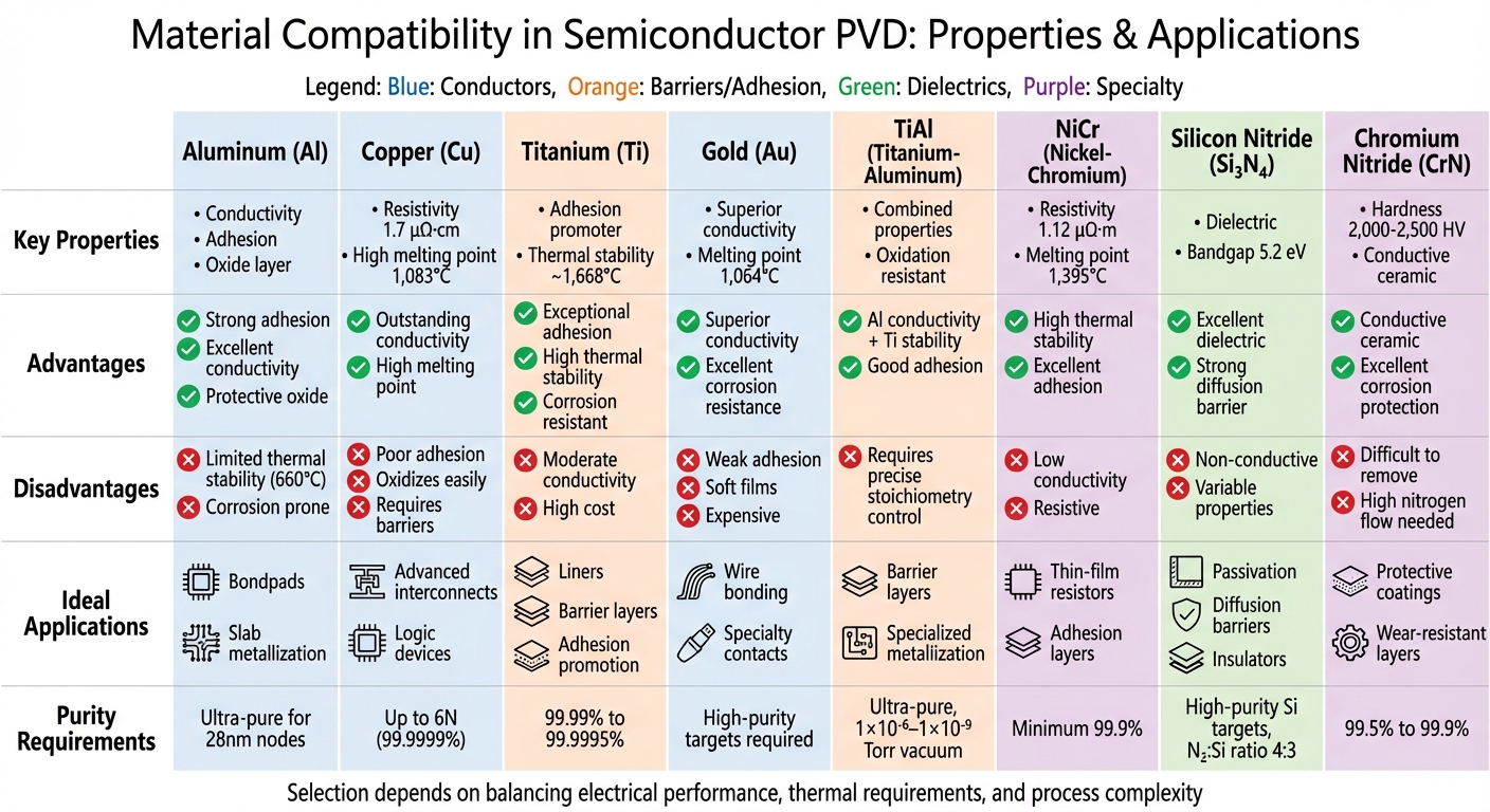
Semiconductor PVD Materials Comparison: Properties and Applications
The following table and discussion offer a concise comparison of the PVD materials previously evaluated in detail.
Each material comes with its own set of strengths and challenges, which play a significant role in determining its suitability for specific applications. Engineers must weigh these trade-offs carefully, considering factors like electrical conductivity, thermal stability, corrosion resistance, and film adhesion. Below is a summary of eight materials, highlighting their key attributes and ideal uses.
| Material | Advantages | Disadvantages | Ideal Uses |
|---|---|---|---|
| Aluminum (Al) | Strong adhesion; excellent conductivity; forms a protective oxide layer | Limited thermal stability (melting point 660°C); prone to corrosion without protective barriers [51] | Bondpads; slab metallization |
| Copper (Cu) | Outstanding electrical conductivity; high melting point (1,083°C) [52] | Poor adhesion; easily oxidizes; requires barrier layers [3][52] | Advanced interconnects; logic devices |
| Titanium (Ti) | Exceptional adhesion; very high thermal stability (~1,668°C); excellent corrosion resistance | Moderate conductivity; relatively high cost | Liners; barrier layers; adhesion promotion |
| Gold (Au) | Superior conductivity; excellent corrosion resistance; high melting point (1,064°C) [52] | Weak adhesion; soft films; expensive | Wire bonding; specialty contacts |
| TiAl (Titanium–Aluminum) | Combines aluminum’s conductivity with titanium’s stability; good adhesion | Requires precise stoichiometry control | Barrier layers; specialized metallization |
| NiCr (Nickel–Chromium) | High thermal stability (melting point 1,395°C) [52]; excellent adhesion | Low conductivity; inherently resistive | Thin-film resistors; adhesion layers |
| Silicon Nitride (Si₃N₄) | Excellent dielectric properties; strong diffusion barrier; high thermal stability | Non-conductive; properties vary with stoichiometry | Passivation; diffusion barriers; insulators |
| Chromium Nitride (CrN) | Conductive ceramic; excellent corrosion protection | Difficult to remove due to chemical inertness; requires high nitrogen flow [40] | Protective coatings; wear-resistant layers |
This table highlights the balance between material properties like conductivity and adhesion. For instance, gold’s excellent conductivity and corrosion resistance make it ideal for niche applications, despite its cost and poor adhesion. Similarly, chromium nitride’s dense structure provides exceptional corrosion protection, but its deposition process demands high nitrogen flow rates [40].
Material purity and precise stoichiometry control are critical for ensuring high-quality films. Ultra-pure metallic and transition-metal nitride films are particularly important for advanced logic and memory devices [3][10]. For example, aluminum’s long-term stability can be significantly improved by plasma-deposited protective films, which enhance resistance to oxygen attack by up to 36 times [51]. Likewise, chromium nitride offers superior protection in aqueous environments, with deposition rates two to three times faster than other materials, despite its demanding process requirements [40].
This information is intended for educational purposes only. Always consult official guidelines and professionals before making sourcing or formulation decisions.
Conclusion
Choosing semiconductor PVD materials involves a careful balance of cost, performance, and reliability. Aluminum remains a popular choice for interconnects and bond pads due to its affordability and ability to perform well within standard temperature ranges. However, engineers must address its vulnerability to electromigration, especially in advanced nodes [1]. For high-performance applications, Copper has become a go-to material, requiring precise integration of barrier layers to ensure durability and efficiency [3]. These examples showcase the trade-offs inherent in PVD processes.
When adhesion and thermal stability are critical, Titanium emerges as a key liner material. Its strong affinity for oxygen ensures excellent adhesion, making it indispensable for creating durable metal–dielectric bonds. For applications needing superior oxidation resistance, such as wire bonding or specialty contacts, Gold provides reliable performance. However, its higher cost means it is typically reserved for critical junctions where long-term reliability outweighs the expense.
The demand for advanced materials is growing, driven by the rise of More-than-Moore applications in power devices and MEMS [6]. Additionally, the PVD coatings market is projected to grow by over 6% annually through 2035, fueled by advancements in packaging technologies like Through Silicon Vias (TSVs) and Re-Distribution Layers (RDLs) [2][5]. To meet these demands, manufacturers should focus on integrated platforms with pre-clean chambers to remove native oxides, ensuring optimal film adhesion and interface quality across all material types [6].
The properties of Aluminum, Copper, Titanium, Gold, TiAl, NiCr, Silicon Nitride, and Chromium Nitride highlight the importance of thoughtful material selection. Ultimately, the choice depends on balancing electrical performance, thermal requirements, and process complexity. Collaborating with equipment providers to determine the best cathode types and deposition methods can ensure consistent results, especially when working with emerging materials like transparent oxide semiconductors [7].
This content is for informational purposes only. Always consult official regulations and qualified professionals before making sourcing or formulation decisions.
FAQs
What challenges arise when using copper in semiconductor PVD processes?
Copper plays a crucial role in semiconductor manufacturing due to its low resistivity, making it ideal for high-performance applications. However, integrating copper through physical vapor deposition (PVD) comes with its own set of challenges. One major issue is agglomeration, which can occur during high-temperature annealing. This problem becomes particularly pronounced when surface impurities, such as oxygen or nitrogen, are present. These impurities can lead to discontinuities in the copper film, increasing resistance and affecting performance. Additionally, as feature sizes shrink below 90 nm, PVD faces step-coverage limitations, often resulting in incomplete seed layers. This can create voids in high-aspect-ratio structures, ultimately impacting yields.
Another challenge with copper is its rapid diffusion into silicon and silicon dioxide, which necessitates the use of robust diffusion barriers. Common materials for these barriers include tantalum (Ta), tantalum nitride (TaN), and titanium nitride (TiN). Even minor defects in these barriers can undermine device reliability, highlighting the importance of precision in their application. Achieving uniform, low-resistivity seed layers also requires high-purity chemicals and meticulous process control, as contaminants can degrade insulation and increase leakage currents.
To address these challenges, Allan Chemical Corporation offers high-purity specialty chemicals specifically designed for barrier-layer deposition, surface cleaning, and copper-seed preparation. These solutions help manufacturers maintain reliability and achieve high-performance results in semiconductor production.
Why is titanium used to improve adhesion in semiconductor layers during PVD processes?
Titanium plays a key role in enhancing adhesion within semiconductor layers by forming robust chemical bonds with oxygen at the interface. These titanium-oxide bonds serve as anchors, firmly securing the PVD film to the dielectric or wafer surface beneath it. This strong attachment is essential for maintaining the stability and reliability of semiconductor devices, ensuring their performance and longevity.
Why is high-purity material essential for PVD in semiconductor manufacturing?
Material purity plays a crucial role in physical vapor deposition (PVD) processes, as even the smallest impurities can cause defects that compromise the performance and reliability of semiconductors. Contaminants, whether present in the source materials or introduced during processing, can alter key thin-film properties such as electrical conductivity, adhesion, and dielectric strength. These changes can lead to problems like inconsistent transistor behavior, higher leakage currents, or even early failure of components.
To address these challenges, the semiconductor industry depends on ultra-high-purity materials, often achieving purity levels as high as 99.999999% (commonly referred to as 8-nines). At these levels, contaminants are reduced to parts-per-billion, minimizing the risk of defects. While high-vacuum environments help control contamination during processing, the feedstock itself must also meet strict purity requirements. Reliable suppliers, such as Allan Chemical Corporation, provide materials that adhere to rigorous purity standards, ensuring they meet the demands of advanced electronic applications.


Comments are closed