Energy Dispersive X-ray Spectroscopy (EDS) is a powerful method for analyzing the elemental composition of nanomaterials with nanometer-scale precision. When paired with Scanning Electron Microscopy (SEM) or Scanning Transmission Electron Microscopy (STEM), it identifies what elements are present and their spatial distribution. EDS works by detecting X-rays emitted as electrons interact with a sample, allowing researchers to map elements across surfaces or within structures.
Key takeaways about EDS mapping:
- How It Works: EDS detects X-rays emitted when an electron beam excites a sample, using these signals to identify elements.
- Applications: Used in semiconductors, batteries, and catalysts to study impurities, surface defects, and active sites.
- Technological Advances: Silicon Drift Detectors (SDDs) improve speed and accuracy, enabling the detection of trace elements in seconds.
- Preparation: Proper sample preparation, like polishing and thin specimen use, ensures accurate results.
- Limitations: Challenges include spectral overlaps, beam damage, and geometry errors, which can be mitigated with advanced techniques and calibration.
This technique is essential for industries like electronics, pharmaceuticals, and materials science, where precise chemical analysis ensures quality and performance. By combining preparation, advanced tools, and reliable materials, EDS delivers detailed insights into nanomaterial composition.
EDS Elemental Mapping Workflow: From Sample Preparation to Data Interpretation
How Is EDS Integrated With Scanning Electron Microscopy (SEM)? – Chemistry For Everyone
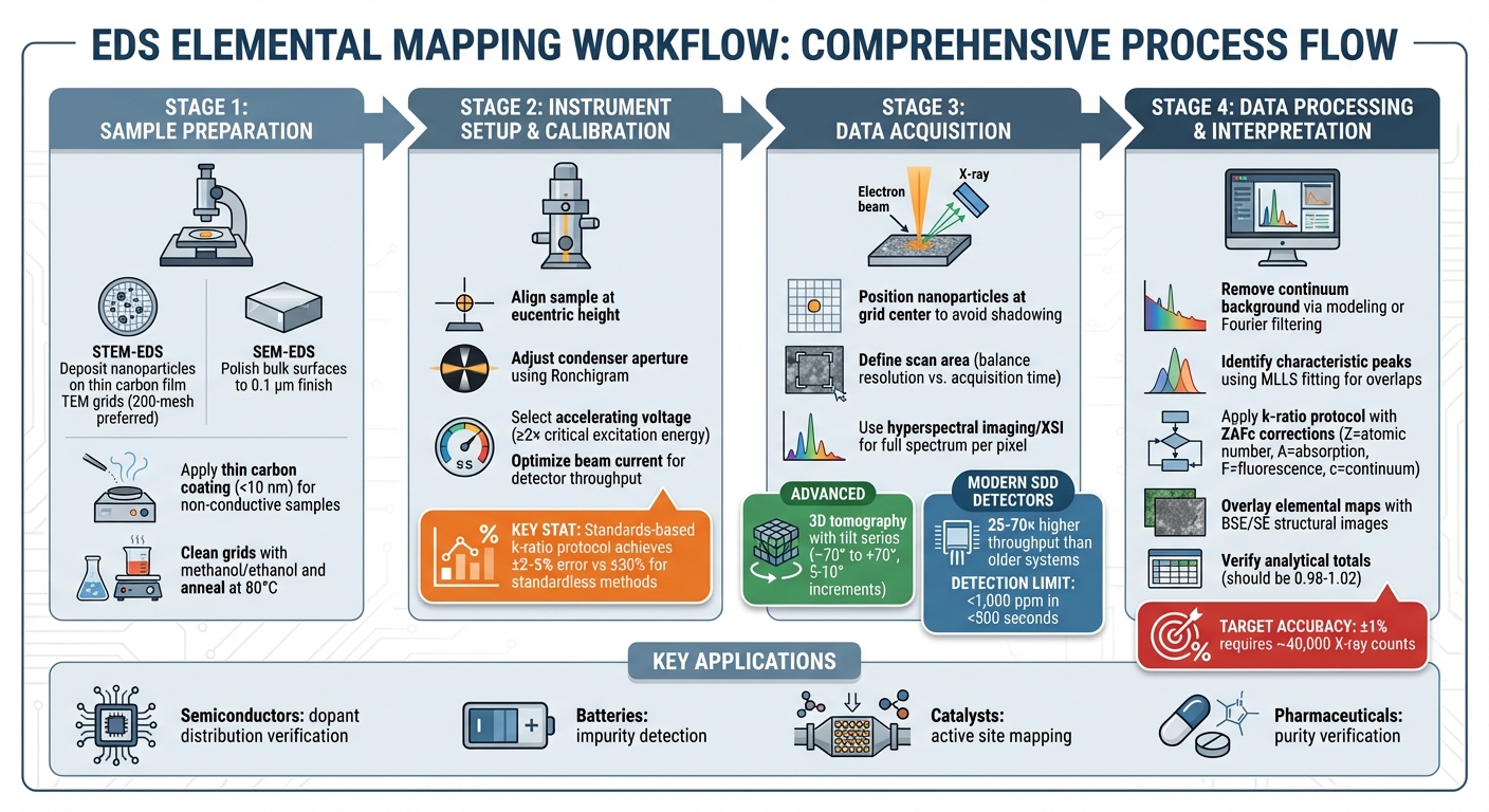
Preparing Nanomaterials and Instruments for EDS Mapping
Accurate preparation of both samples and instruments is crucial for reliable elemental mapping. The approach varies depending on whether you’re conducting SEM-EDS on bulk materials or STEM-EDS on individual nanoparticles. Below is a guide to ensure proper preparation and setup.
Sample Preparation for Nanomaterials
For STEM-EDS, nanoparticles should be deposited onto thin carbon film TEM grids. To minimize interference from spurious X-rays, beryllium grids are preferred, although copper or gold grids can be used if their peaks do not overlap with your sample’s. Opt for 200-mesh grids to avoid interference from grid bars during tomographic mapping. Before use, clean the grids with methanol or ethanol and anneal them in a vacuum at around 80°C (176°F) to reduce contamination [4].
For SEM-EDS, bulk nanomaterial surfaces should be polished to a finish of 0.1 µm or finer. Avoid chemical etching, as it can alter the surface’s topography and composition. For non-conductive samples, apply a thin carbon coating (less than 10 nm) to dissipate charge without obstructing X-ray transmission [6].
Instrument Setup for Nanoscale Analysis
Once the samples are ready, precise instrument calibration is key. Start by aligning the sample at the eucentric height and adjusting the condenser aperture. Use a Ronchigram to correct any aberrations [4]. For accurate quantitative analysis, select an accelerating voltage that excites the desired X-ray lines while keeping the interaction volume minimal. Additionally, optimize the beam current to match the throughput capacity of your detector.
A notable example of proper calibration comes from a study conducted in November 2014 by Dale Newbury and Nicholas Ritchie at NIST. They analyzed NIST Standard Reference Material (SRM) 482, composed of copper–gold alloys, using the k-ratio protocol with a 20 keV beam and standards measured under identical conditions. This approach resulted in relative errors ranging from –1.6% to 1.0%. In contrast, standardless methods produced errors exceeding 20% [6].
Relevance to Regulated Industries
In highly regulated sectors like electronics, ceramics, and pharmaceuticals, even trace impurities (less than 1,000 ppm) can significantly impact performance. Modern SDD-EDS technology can detect these impurities in under 500 seconds [6]. To ensure quality, sourcing high-purity chemicals from trusted suppliers, such as Allan Chemical Corporation, is critical for meeting strict industry standards.
This content is provided for informational purposes only. Always consult official regulations and qualified experts before making sourcing or formulation decisions.
Acquiring High-Resolution Elemental Maps
High-resolution elemental mapping plays a key role in linking the properties of nanomaterials to their performance. To begin collecting elemental data, carefully select scan parameters and, when necessary, use advanced techniques to uncover three-dimensional compositional details.
Step-by-Step Guide to Elemental Map Acquisition
Start by positioning nanoparticles in the center of the grid to avoid shadowing caused by grid bars. This placement ensures visibility at high tilt angles, which is particularly important for detailed analysis. As you search for the ideal location, trace the outline of the grid square to maintain orientation [4]. Define your scan area thoughtfully, balancing spatial resolution with acquisition time. Keep in mind that higher resolutions often require longer scans, which can lead to drift or beam damage in sensitive materials.
Modern SDD-EDS detectors offer much higher throughput compared to their older counterparts while maintaining the same spectral resolution. This is achieved through techniques like hyperspectral imaging or X-ray spectrum imaging (XSI) [2]. These methods capture a full spectrum for every pixel, allowing for retrospective identification of unexpected elements and resolving peak overlaps, such as those between lead and sulfur [5] [9]. Once the sample is positioned correctly, follow these steps to acquire your high-resolution elemental map.
Advanced Techniques: Hyperspectral and 3D Mapping
For a deeper look into internal structures, advanced mapping techniques go beyond standard 2D scans. Traditional two-dimensional EDS maps combine elemental data along the entire electron beam path, which can obscure features like core-shell segregation. Three-dimensional tomography overcomes this limitation by capturing a series of spectrum images while tilting the sample – typically from –70° to +70° in increments of 5° to 10°. The data is then reconstructed using algorithms such as the Simultaneous Iterative Reconstruction Technique (SIRT), which usually requires around 20 iterations for an accurate 3D representation [4].
A 2016 STEM-EDS tomography study highlighted internal compositional gradients in silver-gold nanoparticles, revealing how surface segregation shifts from gold-rich to silver-rich depending on the overall composition [4]. The researchers noted:
"Taking slices through the reconstruction allows the removal of the intensity associated with the top and bottom surfaces of the particles and therefore results in a much clearer display of surface segregation" [4].
One challenge with 3D mapping is detector shadowing. X-ray count intensity can vary with tilt angles due to the sample holder partially blocking the detector. To address this, use a calibration sample, such as a single spherical nanoparticle, before the full scan. Since X-ray counts for a sphere should remain consistent, any variations indicate shadowing that requires correction [4].
Using Live Mapping for Faster Workflows
Live mapping, also known as ESSI, offers a faster and more efficient workflow by collecting multiple fast-frame datasets instead of relying on a single slow serial scan. This process uses the transmitted electron image as a reference for real-time drift correction, ensuring high spatial resolution even during lengthy acquisitions [8]. Additionally, it reduces the instantaneous electron dose, which is essential for protecting beam-sensitive materials like polymers or certain catalysts.
Andrew A. Herzing and Ian M. Anderson from NIST explained:
"The ESSI approach has numerous advantages, most notably the ability to use the relatively strong transmitted electron image signals as a reference to spatially register the sparse XEDS data" [8].
Live mapping allows researchers to quickly identify features of interest and fine-tune acquisition parameters before committing to a lengthy high-resolution scan. This saves valuable time and helps preserve the integrity of delicate samples [8].
This content is provided for informational purposes only. Always consult official regulations and qualified experts before making sourcing or formulation decisions.
sbb-itb-aa4586a
Processing and Interpreting EDS Maps
Turning raw X-ray signals into reliable compositional data is the cornerstone of using EDS (Energy Dispersive Spectroscopy) for mapping elements in nanomaterials. Proper data processing ensures the accuracy needed to unlock the full capabilities of this technique, as previously discussed.
Data Processing for Accurate Elemental Maps
The first step in processing EDS data is removing the continuum background. This can be done through background modeling, which calculates a continuum energy-distribution function along with the detector’s response, or by applying digital filtering methods like Fourier analysis [3]. Once the background is subtracted, the next task is identifying the characteristic peaks that correspond to each element. For complex cases, such as overlapping peaks in materials like PbS, MoS₂, and BaTiO₃, MLLS (Multiple Linear Least Squares) fitting is used to resolve ambiguities [6][7].
To quantify elemental compositions, the k-ratio protocol is applied. This involves comparing the intensity of X-rays from the sample (I₍unknown₎) to those from a standard (I₍standard₎), followed by ZAFc corrections. These corrections account for factors like atomic number effects (Z), X-ray self-absorption (A), secondary fluorescence (F), and continuum contributions (c). When done correctly, this approach achieves a relative error of ±5% in 95% of analyses [6][7]. However, standardless analysis, which skips these corrections, can lead to error margins as wide as ±30% relative [6][7].
Dale E. Newbury and Nicholas W. M. Ritchie from the National Institute of Standards and Technology have cautioned:
"Standardless analysis enables risky analytical behavior with SEM/EDS which contributes enormously to the dismissal of SEM/EDS as being only ‘semi-quantitative’." [6][7]
After processing and quantifying the spectra, the refined data can be correlated with structural images to provide meaningful insights.
Interpreting Elemental Distributions
Once the spectra are processed, the next step is to overlay the elemental maps with structural images, such as Backscattered Electron (BSE) or Secondary Electron (SE) images. This allows for the identification of features like grain boundaries, core-shell structures, and phase distributions [1]. For nanomaterials, traditional 2D maps often combine data along the entire beam path, which can obscure internal details. To overcome this, 3D reconstructions using orthoslices can isolate surface intensity and reveal hidden features like core-shell segregation or compositional gradients [4]. Advanced software can also identify distinct chemical phases, producing high-resolution phase maps instead of simple elemental distributions [1].
Artifacts and Accuracy Considerations
Several factors can affect the accuracy of EDS results. Spectral overlaps are a common issue, often identified by examining the Kα to Kβ intensity ratio, which should approximate 10:1 for energies above 3 keV. Deviations from this ratio may indicate misidentification or the presence of additional elements [3]. Geometric artifacts, such as surface roughness, can alter X-ray path lengths and lead to absorption errors. These errors become apparent when analytical totals fall outside the range of 0.98 to 1.02 [6]. For example, a 2014 NIST study on K411 glass (SRM 470) revealed that polished flat surfaces produced relative errors of –1.1% to 1.8%, whereas fragmented particles caused apparent variations in iron and magnesium concentrations by nearly an order of magnitude [6][7].
To minimize statistical noise, ensure adequate X-ray counts. Modern Silicon Drift Detectors (SDDs) outperform older Si(Li) detectors, offering 25 to 70 times higher X-ray throughput while maintaining excellent spectral resolution [2]. In 3D tomography, detector shadowing caused by the holder or grid bars can lead to variations in X-ray intensity as tilt angles change. This can be corrected using adjusted acquisition times or post-acquisition correction factors [4]. Additionally, verify peak identification by examining all possible excited lines, including weaker ones and artifacts like escape or sum peaks, to ensure no critical data is overlooked [3].
This content is for informational purposes only. Always consult official regulations and qualified experts when making sourcing or formulation decisions.
Practical Strategies and Limitations in Nanoscale EDS Mapping
Optimization Strategies for Nanoscale Accuracy
To achieve dependable results at the nanoscale, careful preparation of samples and proper instrument settings are crucial. Use ultra-thin specimens, ideally around 100 nm thick, to maintain resolution at this scale. Polishing samples to a fine 0.1 µm finish is equally important, as even tiny scratches or surface irregularities can skew elemental data due to absorption effects [6].
Set the accelerating voltage to at least double the critical excitation energy to generate sufficient X-ray intensities [3]. For instance, when analyzing iron (Fe), a voltage of at least 15 kV is required to excite its K lines effectively. Modern Silicon Drift Detectors (SDDs), with throughput rates 25–70 times higher than older systems, allow for faster mapping while maintaining precision [2]. To achieve a statistical accuracy of ±1%, aim to collect roughly 40,000 X-ray counts [3].
For extended acquisition times, live mapping techniques are invaluable. These methods use transmitted electron images for real-time drift correction, preserving high spatial resolution while minimizing the electron dose on beam-sensitive materials [8].
Addressing Limitations in Nanomaterial Mapping
Even with optimized preparation and settings, nanoscale mapping presents inherent challenges. One major issue is low X-ray yields, stemming from the small interaction volumes at this scale. The adoption of Silicon Drift Detectors has significantly improved detection capabilities, achieving sensitivity levels below 0.001 mass fraction (1,000 ppm) within 500 seconds [6]. However, spectral overlaps in complex materials remain a challenge. For example, lead (Pb) M lines can interfere with sulfur (S) K lines. Advanced techniques like Multiple Linear Least Squares (MLLS) fitting help resolve these overlaps effectively [6].
Beam damage is another concern, particularly with sensitive materials. This can be mitigated using techniques like Electron Spread Spectrum Imaging (ESSI), which spreads the electron dose across a larger area, significantly reducing localized damage [8]. In 3D tomography, detector shadowing caused by the sample holder or grid can be addressed by varying acquisition times at different tilt angles or applying corrections based on a calibration specimen, such as a spherical nanoparticle [4].
Specimen geometry is a frequent source of error. Poorly prepared surfaces can lead to concentration readings varying by nearly an order of magnitude [6]. As Dale E. Newbury and Nicholas W. M. Ritchie warned:
"Unless the specimen geometry is carefully controlled, SEM/EDS analysis is subject to errors so broad as to render the compositional results of questionable value for many applications" [6].
Applications in Industrial Chemical Characterization
Accurate elemental mapping is critical in regulated industries to ensure materials meet stringent specifications. Industries such as pharmaceuticals, electronics, and ceramics depend on EDS to verify purity and composition. For example, detecting trace contaminants or confirming the distribution of dopants in semiconductors requires the precision offered by modern SDD-EDS systems. Allan Chemical Corporation, with over 40 years of experience, relies on advanced characterization techniques to guarantee that both technical-grade and compendial-grade chemicals meet exacting standards for use in pharmaceuticals and electronic components.
Standards-based k-ratio protocols are essential for achieving this level of precision. While faster, standardless analysis can lead to relative errors of up to ±30%. In contrast, standards-based methods typically reduce errors to within ±2–5% [6]. The raw analytical total from k-ratio analysis also acts as a quality control metric – totals that deviate significantly from 1.0 (or 100%) often signal geometric issues or the presence of unmeasured elements like oxygen [6]. This degree of accuracy ensures that chemical suppliers can confidently meet the rigorous demands of industries where precise composition is critical to product performance and regulatory compliance. These applications highlight the indispensable role of advanced characterization tools in maintaining industrial chemical quality.
This content is for informational purposes only. Consult official regulations and qualified professionals before making sourcing or formulation decisions.
Conclusion
Key Takeaways
Energy Dispersive Spectroscopy (EDS) has revolutionized nanomaterial characterization by offering nanometer- to atomic-scale resolution. By capturing a complete X-ray spectrum at every pixel, researchers can identify unexpected elements without needing to repeat experiments – a critical advantage in industries like pharmaceuticals, electronics, and ceramics, where detecting contaminants or verifying dopant distributions directly affects product safety and performance [4].
The introduction of modern Silicon Drift Detectors has significantly increased X-ray throughput – up to 70 times higher than older systems – allowing for faster, quantitative mapping. This makes routine quality control more efficient while enabling the detection of trace concentrations as low as 500 ppm [2] [5]. For more complex analyses, EDX tomography provides a three-dimensional view of elemental distributions, overcoming the limitations of traditional 2D projections. For instance, studies on AgAu nanoparticles have demonstrated how surface segregation, influenced by composition, can affect catalytic performance [4].
These advancements highlight the importance of EDS in driving both research progress and quality assurance in highly regulated industries. However, achieving this level of precision relies on proper sample preparation and advanced mapping techniques, as discussed throughout this article.
Role of Reliable Suppliers
Accurate EDS mapping starts with uncontaminated, high-purity feedstocks, making the choice of suppliers crucial. The purity and consistency of starting materials directly impact the reliability of elemental maps, ensuring they reflect true properties rather than artifacts caused by impurities. For example, high-purity precursors like silver nitrate and gold chloride are essential for maintaining synthesis accuracy [10]. Equally important is consistent material morphology, as uniform specimens, such as spherical nanoparticles, are ideal for calibration and correcting detector shadowing during tomographic analysis [10].
Allan Chemical Corporation provides high-purity technical- and compendial-grade chemicals with stringent quality controls. Partnering with trusted suppliers like Allan Chemical ensures reproducible and accurate EDS results, meeting the rigorous standards of industries such as pharmaceuticals, electronics, and advanced materials research. This collaboration between reliable chemical sourcing and advanced EDS techniques continues to drive innovation in nanomaterial science.
This content is for informational purposes only. Always consult official regulations and qualified professionals before making sourcing or formulation decisions.
FAQs
What challenges come with using EDS to analyze nanomaterials?
Energy-dispersive X-ray spectroscopy (EDS) is a widely used method for determining the elemental makeup of nanomaterials, but it’s not without its hurdles. One major challenge is the electron beam’s interaction volume, which can be larger than the nanoparticle itself. This mismatch often leads to interference from the surrounding substrate or nearby particles, ultimately lowering spatial resolution. Another common issue is peak overlap, particularly for lighter elements or those with similar X-ray emission lines, making precise identification and quantification tricky.
Additional difficulties arise from factors like specimen topography, calibration inaccuracies, and the limitations of matrix-correction models, all of which can skew quantitative results. On top of that, practical problems such as low detector efficiency, statistical noise when analyzing trace elements, and beam-induced sample damage can further compromise data quality. To address these challenges, it’s crucial to fine-tune beam settings, carefully prepare samples, and apply meticulous data processing techniques to ensure dependable outcomes.
Why is proper sample preparation important for accurate EDS mapping?
Proper sample preparation plays a key role in ensuring accurate results during EDS (Energy Dispersive Spectroscopy) mapping. The condition of the sample surface directly influences how X-rays are generated and detected. A surface that is clean, flat, and conductive helps minimize issues like charging and beam scattering, which can lead to errors in determining the sample’s elemental composition.
Techniques such as mechanical polishing, ion milling, or focused-ion-beam thinning should be chosen with care to maintain the integrity of the sample’s nanostructure while effectively removing surface contaminants. For nanomaterials, even a thin polymer coating can interfere with detecting light elements. Using high-purity conductive coatings, such as carbon or gold, can significantly improve charge dissipation and enhance signal clarity.
Allan Chemical Corporation supplies the high-purity chemicals and coating materials needed for these critical preparation steps. By optimizing sample preparation, laboratories can achieve highly accurate EDS measurements, often within a margin of ±2% for well-prepared samples.
What recent advancements have enhanced the speed and precision of EDS mapping for nanomaterials?
Advances in Energy Dispersive Spectroscopy (EDS) have dramatically increased its speed and accuracy in mapping elements within nanomaterials. Among these breakthroughs are silicon-drift detectors, which improve the efficiency of X-ray detection, and event-streamed spectrum-imaging (ESSI), a technology that enables the rapid collection of high-resolution data across multiple frames.
The combination of high-current, atom-sized electron probes and ultra-sensitive X-ray detectors has pushed the boundaries of elemental analysis, making it possible to study materials at the atomic level with incredible detail. Additionally, fast STEM spectrum-imaging techniques have simplified the process, delivering precise elemental maps in significantly less time. These developments have solidified EDS as an essential tool for examining intricate nanostructures with unparalleled precision and speed.


Comments are closed